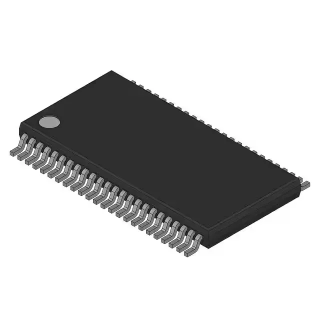
Infineon Technologies CY2SSTV850ZC — Clock & Timing ICs

CY2SSTV850ZC PLL Clock Driver, 170 MHz, 1:10 SSTL-2

MPNCY2SSTV850ZC
End of Life

Cypress CY2SSTV850ZC, PLL-based clock driver, SSTV series, 1 circuit, 1:10 input:output, 170 MHz max, differential I/O, SSTL-2 output, 2.375 V to 3.465 V supply, 0°C to 70°C, 48-TSSOP.

$2.01Ref. price · indicative, final on quote
Packaging48-TFSOP (0.240", 6.10mm Width)
StockContact for availability
MOQ1 pcs
  • 100% new & originalTraceable channels only — no refurbs, no pulls, no remarked parts.
  • Date & lot codes on quoteStated per line before you commit; label photos on request.
  • MSL-compliant ESD packingMoisture-sealed bags with indicator cards; reels photo-verified.
  • PayPal buyer protectionPay by T/T, PayPal or Payoneer — card payments covered end to end.

Specifications

CY2SSTV850ZC Technical Specifications
ParameterValue
Mounting typeSurface Mount
Voltage2.375V ~ 3.465V
Frequency170MHz
Operating temperature0°C ~ 70°C
PLLYes with Bypass
InputClock
OutputSSTL-2
PackageBulk
Case48-TFSOP (0.240\", 6.10mm Width)
Divider (Multiplier)No/No
Number of circuits1
Ratio - Input:Output1:10
Differential - Input:OutputYes/Yes

Product details

PLL clock buffer for DDR memory buses

The Cypress CY2SSTV850ZC is a PLL-based clock driver that distributes a single reference clock to up to ten SSTL-2 loads.

Differential I/O and PLL bypass

Both the input and outputs are differential (Yes/Yes per the spec), which improves noise immunity and reduces electromagnetic emissions compared to single-ended clock distribution. The PLL can be bypassed (Yes with Bypass), allowing the input clock to pass through to the outputs with minimal added jitter — useful for system test modes or when the PLL's frequency multiplication is not needed. The part does not include an internal divider or multiplier (No/No).

Lifecycle and compliance

The part is marked RoHS non-compliant. For designs targeting EU RoHS or similar regulations, a lead-free equivalent should be evaluated.

Sourcing posture

Given the active lifecycle and RoHS constraint, the buyer should confirm the acceptable compliance level for the target market before committing the BOM line.

Frequently asked questions

What is the output type of CY2SSTV850ZC?

The output type is SSTL-2, the JEDEC standard for DDR SDRAM clock inputs. Both the input and outputs are differential.

Is CY2SSTV850ZC RoHS compliant?

No, CY2SSTV850ZC is marked RoHS non-compliant. For designs requiring RoHS compliance, evaluate a lead-free equivalent such as the CY2SSTV850ZXC or a newer family member.

What is the closest functional alternative to CY2SSTV850ZC?

A functional alternative is the CY2305SXI-1HT, a fanout buffer / zero delay buffer with 1:5 fanout, 133.33 MHz max frequency, single-ended I/O, and 3.0 V supply in a smaller package. The CY2SSTV850ZC offers higher fanout (1:10), differential I/O, and SSTL-2 output, making it more suited for DDR memory clock distribution than the CY2305.

What are the specifications of CY2SSTV850ZC?

Key specifications include: PLL with bypass, 170 MHz max frequency, 1:10 input-to-output ratio, differential input and output, SSTL-2 output, 2.375 V to 3.465 V supply, 0°C to 70°C operating temperature, 48-TSSOP package, surface mount.