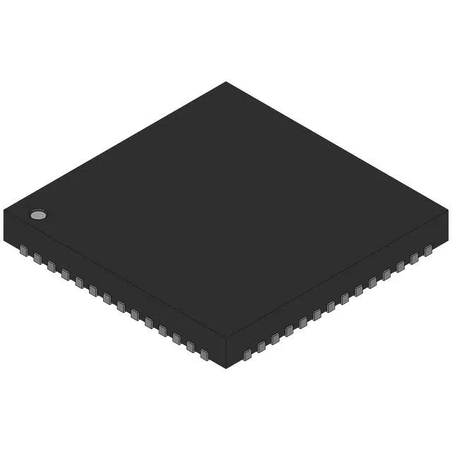
280 MHz D-Type flip-flop in 56-QFN-EP
The CY2SSTV16859LFCT: That 5 ns window sets the data-rate ceiling for the downstream logic — the output rise time into the 30 pF load adds to this, so the actual toggle rate at the receiver is lower than the bare clock suggests. The exposed pad also provides a low-inductance ground return for the 16 mA per-pin output drive — critical when terminating DDR address/control lines.
Supply and output drive
Operates from a 2.3 V to 2.7 V supply with a quiescent current of 40 mA. The tight 400 mV window means the rail must be regulated — a 2.5 V LDO with ±2% tolerance keeps the part inside its envelope even under load transients from the 16 mA per-pin output drive. Both positive- and negative-edge trigger inputs are available, and the output is non-inverted with a reset function. The 3.5 pF input capacitance per pin is low enough for high-speed clock distribution but still contributes to the total load on the driving source — budget it into the fan-out calculation.
The part is RoHS non-compliant per the manufacturer's declaration — verify your assembly line's exemption allowance for lead-bearing finishes before committing the BOM.