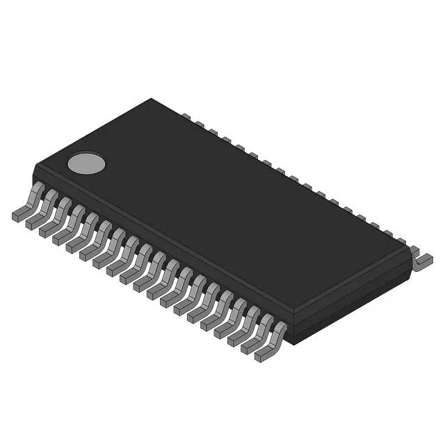
Infineon Technologies CY2DP818ZXC — Discrete Semiconductors

CY2DP818ZXC Fanout Buffer, 350 MHz, 1:8, 38-TSSOP

MPNCY2DP818ZXC
End of Life

Cypress CY2DP818ZXC Fanout Buffer (Distribution), 350 MHz, 1:8 LVDS/LVPECL/LVTTL input to LVPECL output, 38-TFSOP (0.173", 4.40mm Width), 38-TSSOP, Surface Mount, Bulk.

$4.46Ref. price · indicative, final on quote
Packaging38-TFSOP (0.173", 4.40mm Width)
RoHSROHS3 Compliant
Independent supplier — new & surplus stockAuthenticity-screened · ESD-safe packingListing updated Aug 2026

Specifications

CY2DP818ZXC specifications
ParameterValue
TypeFanout Buffer (Distribution)
MountingSurface Mount
Supply voltage3.135V ~ 3.465V
Frequency - max350 MHz
Operating temperature0°C ~ 70°C (TA)
InputLVDS, LVPECL, LVTTL
OutputLVPECL
PackageBulk
Case38-TFSOP (0.173\", 4.40mm Width)
Number of circuits1
Ratio - Input:Output1:8
Differential - Input:OutputYes/Yes

Product details

Clock fanout for high-speed differential lines

The CY2DP818ZXC is a 1:8 fanout buffer that takes a single differential input (LVDS, LVPECL, or LVTTL) and distributes eight LVPECL copies with low skew — the part is described as a LOW SKEW CLOCK DRIVER. It handles clock frequencies up to 350 MHz, which covers most high-speed SERDES reference clocks, FPGA fabric clocks, and data-converter sample clocks in the 100–300 MHz range.

Signal compatibility and supply

The input accepts LVDS, LVPECL, or LVTTL levels, so it can sit behind a PLL output, an oscillator, or a backplane clock without a separate level translator. Outputs are LVPECL — the differential swing is about 800 mV peak-to-peak, which drives terminated 50-Ohm lines directly.

Frequently asked questions

What input signal types does CY2DP818ZXC accept?

It accepts LVDS, LVPECL, and LVTTL inputs and outputs LVPECL, making it flexible for interfacing with common high-speed clock sources.