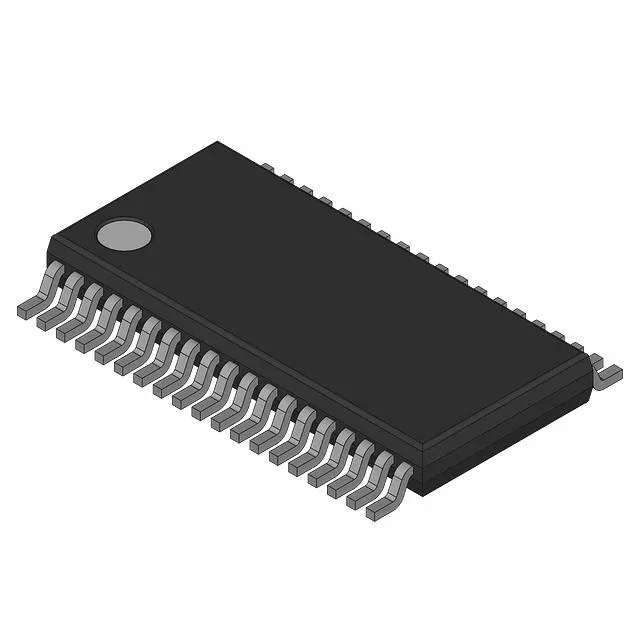
Infineon Technologies CY2DP818ZI-2 — Analog & Data Acquisition

CY2DP818ZI-2 Fanout Buffer, 350 MHz, 1:8 LVPECL Output

MPNCY2DP818ZI-2
End of Life

Cypress Semiconductor CY2DP818ZI-2, Fanout Buffer (Distribution) low skew clock driver, 1:8 ratio, 350 MHz max, LVDS/LVPECL/LVTTL input, LVPECL output, 38-TFSOP (0.173", 4.40mm Width) Surface Mount, -40°C to 85°C.

$5.74Ref. price · indicative, final on quote
Packaging38-TFSOP (0.173", 4.40mm Width)
StockContact for availability
MOQ1 pcs
  • 100% new & originalTraceable channels only — no refurbs, no pulls, no remarked parts.
  • Date & lot codes on quoteStated per line before you commit; label photos on request.
  • MSL-compliant ESD packingMoisture-sealed bags with indicator cards; reels photo-verified.
  • PayPal buyer protectionPay by T/T, PayPal or Payoneer — card payments covered end to end.

Specifications

CY2DP818ZI-2 Technical Specifications
ParameterValue
TypeFanout Buffer (Distribution)
Mounting typeSurface Mount
Voltage3.135V ~ 3.465V
Frequency350 MHz
Operating temperature-40°C ~ 85°C (TA)
InputLVDS, LVPECL, LVTTL
OutputLVPECL
PackageBulk
Case38-TFSOP (0.173\", 4.40mm Width)
Number of circuits1
Ratio - Input:Output1:8
Differential - Input:OutputYes/Yes

Product details

What this CY2DP818ZI-2 fanout buffer does on your clock tree

The Cypress CY2DP818ZI-2 is a low skew clock driver — a fanout buffer, not a PLL or jitter cleaner. It takes one clock input and distributes it to eight LVPECL outputs with minimal added skew between channels. That 1:8 ratio means a single device can feed eight destination ICs from one source, saving board space versus daisy-chaining multiple smaller buffers. Input flexibility covers LVDS, LVPECL, and LVTTL, so it can sit behind an oscillator, a PLL output, or a logic-level clock source without extra level translation. Outputs are differential LVPECL, the standard for high-speed clock distribution in telecom and data-comm systems where noise margin matters. Rated for 350 MHz maximum frequency. The differential input and output path gives common-mode rejection on the input side, which helps when the clock source is across a backplane or cable.

Supply rails and temperature — where this part lives

Supply range is 3.135 V to 3.465 V. The industrial temperature grade of -40°C to 85°C covers outdoor telecom cabinets, factory floor enclosures, and base station equipment where the ambient isn't climate-controlled. Package is a 38-TSSOP, body width 4.40 mm. The single-circuit design means one buffer per package; no dual or quad options to confuse the BOM.

Lifecycle and sourcing reality

The RoHS status shows non-compliant. For RoHS-mandated builds, you'll need to check if an equivalent RoHS-compliant variant exists in the family.

Frequently asked questions

What input and output types does CY2DP818ZI-2 support?

The CY2DP818ZI-2 accepts LVDS, LVPECL, or LVTTL inputs and provides eight LVPECL outputs. The differential input and output path gives common-mode noise rejection on the input side, important when the clock source is remote.

What is the maximum frequency of CY2DP818ZI-2?

The CY2DP818ZI-2 is rated for a maximum frequency of 350 MHz, suitable for distributing telecom reference clocks and high-speed FPGA fabric clocks.