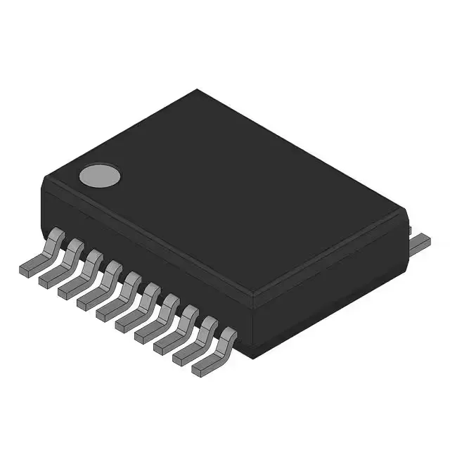
Infineon Technologies CY2CC910OIT — Analog & Data Acquisition

CY2CC910OIT Fanout Buffer, 650 MHz, 1:10, 20-SSOP

MPNCY2CC910OIT
End of Life

Infineon (Cypress) CY2CC910OIT, Fanout Buffer (Distribution), 1:10 ratio, 650 MHz max, AVCMOS input/output, 1.71V-3.3V supply, -40°C to 85°C, 20-SSOP package, Surface Mount.

$2.07Ref. price · indicative, final on quote
Packaging20-SSOP (0.209", 5.30mm Width)
StockContact for availability
MOQ1 pcs
  • 100% new & originalTraceable channels only — no refurbs, no pulls, no remarked parts.
  • Date & lot codes on quoteStated per line before you commit; label photos on request.
  • MSL-compliant ESD packingMoisture-sealed bags with indicator cards; reels photo-verified.
  • PayPal buyer protectionPay by T/T, PayPal or Payoneer — card payments covered end to end.

Specifications

CY2CC910OIT Technical Specifications
ParameterValue
TypeFanout Buffer (Distribution)
Mounting typeSurface Mount
Voltage1.71V ~ 3.3V, 2.375V ~ 3.3V, 3.135V ~ 3.3V
Frequency650 MHz
Operating temperature-40°C ~ 85°C
InputAVCMOS
OutputAVCMOS
PackageBulk
Case20-SSOP (0.209\", 5.30mm Width)
Number of circuits1
Ratio - Input:Output1:10
Differential - Input:OutputNo/No

Product details

650 MHz 1:10 low-skew clock distribution

The Infineon (Cypress) CY2CC910OIT is a 1:10 fanout buffer designed to distribute a single AVCMOS clock input to ten outputs with low skew. It handles clock frequencies up to 650 MHz, making it suitable for high-speed timing distribution in telecom, networking, and data-communications equipment where maintaining signal integrity across multiple branches matters. The part operates from a 1.71V to 3.3V supply range, with additional narrower windows of 2.375V to 3.3V and 3.135V to 3.3V, giving flexibility when interfacing with different logic families. The input and output are both single-ended AVCMOS — no differential signaling — so it fits designs using standard CMOS clock sources rather than LVPECL or LVDS.

What the supply voltage ranges mean for your BOM

The CY2CC910OIT lists three overlapping supply ranges: 1.71V to 3.3V, 2.375V to 3.3V, and 3.135V to 3.3V. This is not a mistake — it reflects the device's ability to operate across different voltage domains depending on the input signal swing and output load. The widest range (1.71V to 3.3V) covers low-voltage cores down to 1.8V logic, while the tighter windows ensure proper switching thresholds at higher supply levels. For a BOM running a 3.3V clock tree, any of the three ranges works; for a 1.8V I/O bank, only the 1.71V to 3.3V window applies. Plan the supply rail accordingly and confirm the input voltage meets the AVCMOS thresholds at your chosen VDD.

The 20-SSOP package (0.209" body width, 5.30 mm) is a surface-mount footprint common in moderate-density designs.

Lifecycle and compliance note

If your assembly line requires RoHS-10 exemption or full lead-free processing, verify the exemption status or look for a lead-free variant suffix. For defense, aerospace, or high-reliability applications where leaded finish is preferred, this is actually an advantage.

Frequently asked questions

Does CY2CC910OIT support differential inputs?

No. The CY2CC910OIT has single-ended AVCMOS input and output only — differential input and output are both marked "No/No". It is not compatible with LVPECL, LVDS, or HCSL clock sources without external level translation.

How many outputs does CY2CC910OIT provide?

The CY2CC910OIT provides ten outputs from a single input, for a 1:10 fanout ratio. This is a single-circuit device (one buffer channel) driving all ten outputs.

What is the maximum frequency of CY2CC910OIT?

The CY2CC910OIT supports clock frequencies up to 650 MHz maximum. This is the upper limit for the AVCMOS input; actual achievable frequency depends on supply voltage, load capacitance, and signal integrity on the PCB.