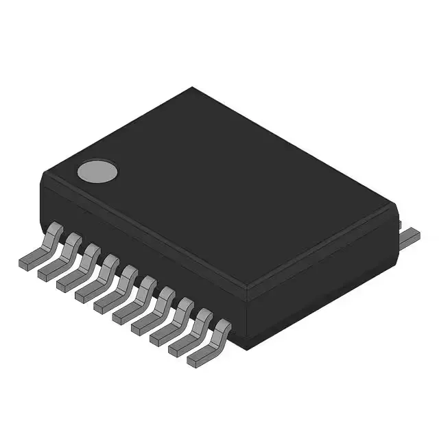
What this clock buffer does on the board
The Cypress CY2CC810OI is a low skew clock driver — a fanout buffer that takes one LVCMOS input and distributes it to ten AVCMOS outputs with minimal skew between them. That 1:10 ratio means a single reference clock from an oscillator or FPGA can feed ten downstream loads — PLLs, SERDES reference inputs, or multiple ASICs — without loading the source. The part handles up to 650 MHz, so it belongs in high-speed digital boards: Ethernet switches, baseband processors, or any design where clock distribution needs clean edges and matched delays.
Temperature grade and where it goes
If you are repairing a board that lives in a warm enclosure or sees seasonal temperature swings, the CY2CC810OI holds its skew specs across that span.
Housed in a 20-pin SSOP (5.30 mm body width), surface-mount. The 0.209" (5.30 mm) width is a standard SSOP footprint — no exotic land pattern. If you are replacing a failed buffer on a production board, verify the existing footprint matches this package; the 20-SSOP is common enough that layout should be straightforward.