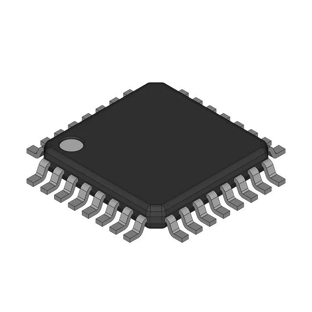
Infineon Technologies CY29658AI — Clock & Timing ICs

CY29658AI Zero Delay Buffer – Infineon, LVPECL Input

MPNCY29658AI
End of Life

Infineon CY29658AI Zero Delay Buffer, PLL-based clock driver, LVPECL input, LVCMOS outputs, 1:10 fanout, 200 MHz max, 32-TQFP (7x7), -40°C to 85°C, dual supply 2.375V–2.625V / 3.135V–3.465V

$5.14Ref. price · indicative, final on quote
Packaging32-TQFP
StockContact for availability
MOQ1 pcs
  • 100% new & originalTraceable channels only — no refurbs, no pulls, no remarked parts.
  • Date & lot codes on quoteStated per line before you commit; label photos on request.
  • MSL-compliant ESD packingMoisture-sealed bags with indicator cards; reels photo-verified.
  • PayPal buyer protectionPay by T/T, PayPal or Payoneer — card payments covered end to end.

Specifications

CY29658AI Technical Specifications
ParameterValue
TypeZero Delay Buffer
Mounting typeSurface Mount
Voltage2.375V ~ 2.625V, 3.135V ~ 3.465V
Frequency200 MHz
Operating temperature-40°C ~ 85°C (TA)
InputLVPECL
OutputLVCMOS
PackageBulk
Case32-TQFP
Number of circuits1
Ratio - Input:Output1:10
Differential - Input:OutputYes/No

Product details

Zero delay buffer with LVPECL input and 1:10 LVCMOS fanout

The CY29658AI is a PLL-based zero delay buffer from Infineon that accepts a single LVPECL input and distributes it to ten LVCMOS outputs with matched edge placement. The 200 MHz maximum frequency covers most FPGA, ASIC, and processor clock trees in telecom, networking, and industrial control equipment.

Supply flexibility and temperature grade

Operates from either a 2.5V rail (2.375V to 2.625V) or a 3.3V rail (3.135V to 3.465V), letting the same BOM position serve designs with different core voltages.

Package and footprint for layout planning

Housed in a 32-TQFP with a 7x7 mm body (supplier device package 32-TQFP (7x7)). The 0.80 mm pitch is routable on a four-layer board without blind vias; the exposed pad (if present) should be stitched to ground plane with at least nine thermal vias to keep the PLL junction temperature within spec.

Lifecycle and compliance posture

The part is RoHS non-compliant, so designs destined for EU or similar markets may need an exemption or a lead-free alternative.

Frequently asked questions

What is the input and output logic of CY29658AI?

The input is LVPECL (differential) and the outputs are single-ended LVCMOS. The input:output ratio is 1:10.

Is CY29658AI RoHS compliant?

No, it is listed as RoHS non-compliant. Verify your market's exemption rules or consider a lead-free alternative if required.