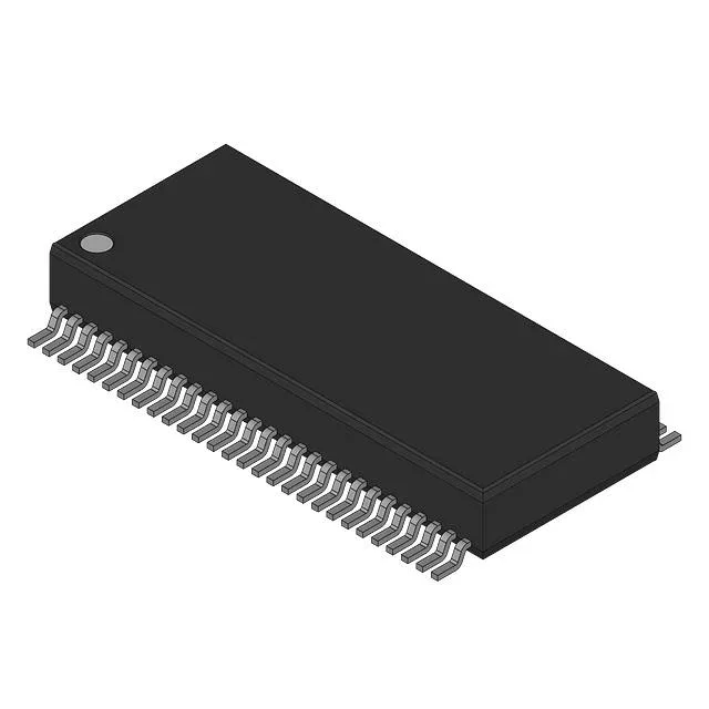
Infineon Technologies CY28341OC-2 — Discrete Semiconductors

CY28341OC-2 PLL Clock Buffer, 200 MHz, 1:20, DDR, 56-SSOP

MPNCY28341OC-2
End of Life

Cypress CY28341OC-2 PLL clock buffer, 200 MHz max, 1:20 input:output ratio, differential outputs, 56-SSOP, 0°C to 70°C, RoHS non-compliant.

$3.13Ref. price · indicative, final on quote
Packaging56-BSSOP (0.295", 7.50mm Width)
StockContact for availability
MOQ1 pcs
  • 100% new & originalTraceable channels only — no refurbs, no pulls, no remarked parts.
  • Date & lot codes on quoteStated per line before you commit; label photos on request.
  • MSL-compliant ESD packingMoisture-sealed bags with indicator cards; reels photo-verified.
  • PayPal buyer protectionPay by T/T, PayPal or Payoneer — card payments covered end to end.

Specifications

CY28341OC-2 Technical Specifications
ParameterValue
Mounting typeSurface Mount
Voltage2.375V ~ 2.375V, 3.135V ~ 3.135V
Frequency200MHz
Operating temperature0°C ~ 70°C (TA)
PLLYes
InputCrystal
OutputClock
PackageBulk
Main purposeDDR
Case56-BSSOP (0.295\", 7.50mm Width)
Number of circuits2
Ratio - Input:Output1:20
Differential - Input:OutputNo/Yes

Product details

What this PLL clock buffer does for a DDR board

The CY28341OC-2 is a PLL-based clock buffer from Cypress, built to take a single crystal input and fan it out to 20 clock outputs at up to 200 MHz. It is aimed squarely at DDR memory clock trees — the 1:20 ratio means one crystal reference can feed the whole DIMM slot array without daisy-chaining a second buffer. Outputs are differential (No/Yes on the input/output side), which is what DDR interfaces expect for clean edge rates and low jitter on the rising edge.

Temperature range and where it fits

Rated 0°C to 70°C, this is a commercial-temperature part. It belongs in a desktop motherboard, a server blade, or a telecom line card in a conditioned room — not in an engine bay, a rooftop enclosure, or a factory floor without climate control. If your BOM calls for industrial temp, this is not the part.

Package and mounting

56-pin SSOP, 7.50 mm body width, surface-mount. The 0.295-inch-wide footprint is standard for this density. Orientation is marked by pin 1 chamfer on the package — no ambiguity on a pick-and-place line or a rework station. No special handling beyond normal ESD precautions.

Lifecycle and sourcing reality

Listed as Active in production. It is RoHS non-compliant.

Frequently asked questions

Is CY28341OC-2 compatible with VIA P4 chipset?

The description lists it as a frequency timing generator for VIA P4 chipsets. It is designed to generate the clock signals required by that chipset family.

What is the max frequency of CY28341OC-2?

The maximum output frequency is 200 MHz, which covers DDR-200, DDR-266, and DDR-333 memory clock rates.