Infineon Technologies CY27410FLTXI — Logic ICs

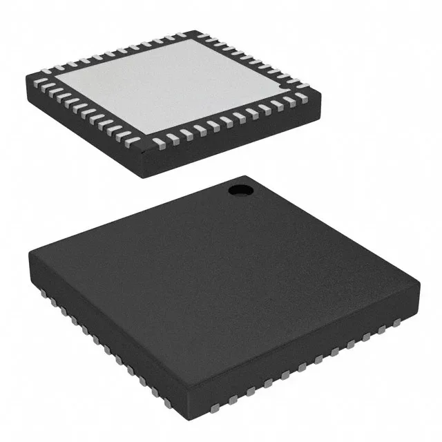
CY27410FLTXI Clock Generator, 700 MHz, 48-QFN

MPNCY27410FLTXI
End of Life

Infineon CY27410FLTXI clock generator IC, PLL with bypass, 700 MHz max frequency, 3:12 input-to-output ratio, outputs CML/HCSL/LVCMOS/LVDS/LVPECL, 48-VFQFN exposed pad, -40°C to 85°C, active lifecycle.

$33.02Ref. price · indicative, final on quote
Packaging48-VFQFN Exposed Pad
StockContact for availability
MOQ1 pcs
  • 100% new & originalTraceable channels only — no refurbs, no pulls, no remarked parts.
  • Date & lot codes on quoteStated per line before you commit; label photos on request.
  • MSL-compliant ESD packingMoisture-sealed bags with indicator cards; reels photo-verified.
  • PayPal buyer protectionPay by T/T, PayPal or Payoneer — card payments covered end to end.

Specifications

CY27410FLTXI Technical Specifications
ParameterValue
Mounting typeSurface Mount
Voltage1.71V ~ 3.46V
Frequency700MHz
Operating temperature-40°C ~ 85°C
PLLYes with Bypass
InputLVCMOS, Crystal
OutputCML, HCSL, LVCMOS, LVDS, LVPECL
PackageTray
Case48-VFQFN Exposed Pad
Divider (Multiplier)No/No
Number of circuits1
Ratio - Input:Output3:12
Differential - Input:OutputYes/Yes

Product details

700 MHz PLL clock generator with programmable output types

The Infineon CY27410FLTXI is a single-circuit PLL-based clock generator with bypass mode, capable of synthesizing up to 700 MHz on its outputs. It accepts LVCMOS or crystal inputs and can deliver CML, HCSL, LVCMOS, LVDS, or LVPECL levels — covering the major high-speed signaling standards used in SerDes reference clocks, FPGA transceiver banks, and Ethernet PHY interfaces. The 3:12 input-to-output ratio allows three independent clock sources to be fanned out to twelve loads, which simplifies clock trees in multi-ASIC or multi-card systems where each input may drive a different frequency domain.

Package and footprint notes

Housed in a 48-VFQFN with exposed pad (7x7 mm body). MSL 3 out of the bag; bake before reflow if the moisture-barrier bag has been open past the floor-life window.

Frequently asked questions

What output types does CY27410FLTXI support?

The device outputs CML, HCSL, LVCMOS, LVDS, and LVPECL levels. This range covers the common high-speed signaling standards used in SerDes, FPGA, and Ethernet clock distribution.

What is the maximum frequency of CY27410FLTXI?

The maximum output frequency is 700 MHz, making it suitable for clocking high-speed SerDes transceivers, FPGA reference clocks, and 10 GbE PHYs.