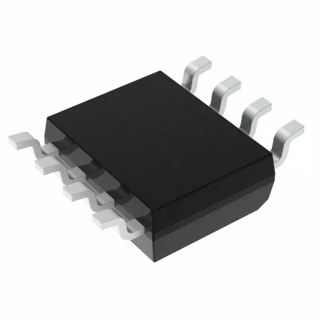
Infineon Technologies CY25100SXIF — Clock & Timing ICs

CY25100SXIF PLL Clock Generator – Infineon, 200 MHz, 8-SOIC

MPNCY25100SXIF
End of Life

Infineon CY25100SXIF, PLL-based fanout buffer and spread-spectrum clock generator, 200 MHz max output, 1:2 CMOS fanout, 3.13 V to 3.45 V supply, industrial temperature range, 8-SOIC package.

$13.36Ref. price · indicative, final on quote
Packaging8-SOIC (0.154", 3.90mm Width)
StockContact for availability
MOQ1 pcs
  • 100% new & originalTraceable channels only — no refurbs, no pulls, no remarked parts.
  • Date & lot codes on quoteStated per line before you commit; label photos on request.
  • MSL-compliant ESD packingMoisture-sealed bags with indicator cards; reels photo-verified.
  • PayPal buyer protectionPay by T/T, PayPal or Payoneer — card payments covered end to end.

Specifications

CY25100SXIF Technical Specifications
ParameterValue
TypeFanout Buffer (Distribution), Spread Spectrum Clock Generator
Mounting typeSurface Mount
Voltage3.13V ~ 3.45V
Frequency200MHz
Operating temperature-40°C ~ 85°C
PLLYes
InputCMOS, Crystal
OutputCMOS
PackageTube
Case8-SOIC (0.154\", 3.90mm Width)
Divider (Multiplier)Yes/No
Number of circuits1
Ratio - Input:Output1:2
Differential - Input:OutputNo/No

Product details

What this clock IC does in the timing tree

The CY25100SXIF is a single-circuit PLL that accepts a CMOS or crystal input and produces two CMOS outputs at up to 200 MHz. The integrated spread-spectrum modulation reduces peak EMI on the output clock — useful when the board must pass radiated-emissions testing without a metal shield. The 1:2 fanout ratio means one input drives two output traces; the PLL cleans up jitter from the source and re-times the edges. Because the part lacks differential outputs, it targets single-ended CMOS clock trees — not LVDS or LVPECL backplanes.

Supply rail and temperature — what to budget

The supply range is 3.13 V to 3.45 V — a 3.3 V nominal rail with ±4 % tolerance. A standard 3.3 V ±10 % rail (2.97 V to 3.63 V) exceeds the upper limit; use a regulated 3.3 V LDO or a switcher with tight setpoint to stay inside the window. The 8-SOIC package (3.90 mm width) is a common footprint; the SOIC-8 land pattern matches standard IPC-7351 guidelines.

Frequently asked questions

What is the difference between CY25100SXIF and CY25100SXI?

The suffix 'F' on CY25100SXIF indicates ROHS3 compliance (lead-free). The CY25100SXI variant (without 'F') is the non-ROHS version. Electrically the two are identical — same PLL, same 200 MHz limit, same 8-SOIC package. If your BOM requires ROHS3, the 'F' suffix is the correct order code.

When sourcing CY25100SXIF, what's the closest functional second-source — CY2305SXI-1HT?

The CY2305SXI-1HT is a PLL-based fanout buffer from the same Infineon family, but it is not a pin-for-pin drop-in. The CY2305 has a 1:5 fanout ratio (vs 1:2 on the CY25100), a 133.33 MHz max frequency (vs 200 MHz), and a different supply voltage range (3.0 V nominal vs 3.13–3.45 V). It also lacks spread-spectrum modulation. For a direct replacement, stick with the CY25100SXIF.