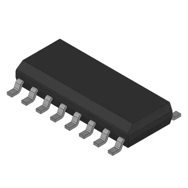
What this PLL clock buffer does on your board
The CY23S08SI-1H is a PLL-based zero-delay buffer that takes a single LVCMOS or LVTTL input and distributes it to eight LVCMOS outputs with near-zero skew. The internal PLL can also be bypassed, letting you use it as a simple fanout buffer when you don't need the phase alignment. Maximum output frequency is 140 MHz, which covers most microcontroller, FPGA, and memory-bus clock trees below that ceiling. The 1:8 ratio means one input drives eight loads — handy when you've got multiple peripherals sharing a single clock source.
Supply, temperature, and package fit
Housed in a 16-SOIC (3.90 mm width) package — a hand-solderable footprint that's also easy to inspect under a microscope. Lifecycle status is Active, meaning Infineon still produces it and it's available for new designs. RoHS compliance is listed as non-compliant, so if your BOM requires RoHS, you'll need to verify the specific date-code or look for a lead-free variant.