Clock distribution with PLL bypass — what this part does
The Cypress CY23FS08OC is a zero delay buffer from the Failsafe™ family, designed to regenerate a clean clock from a jittery source or pass a clean clock straight through. It integrates a PLL with bypass capability, so you can either let the PLL clean up the incoming clock or bypass it entirely and feed the reference directly to the outputs. The part accepts LVCMOS, LVTTL, or crystal inputs and delivers LVCMOS outputs at up to 200 MHz. With a 3:8 input-to-output ratio, it fans out three clock inputs to eight outputs — useful for distributing a system clock across multiple loads on a single board.
Supply rails and temperature — fit check for the BOM
The device operates from a 2.375 V to 2.625 V rail or a 3.135 V to 3.465 V rail.
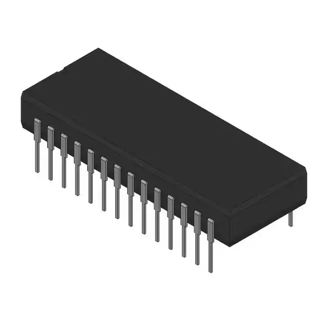
Housed in a 28-pin SSOP with a 0.209-inch body width and 5.30 mm width, surface-mount. The 28-SSOP footprint is common enough that board layout is straightforward, but the tight pitch means solder-paste inspection is worth a pass on first build.
RoHS status — compliance matters
This part is RoHS non-compliant. If your BOM requires RoHS compliance, the CY23FS08OC will not pass the bill of materials audit. That is a hard gate for many production lines, especially in consumer or medical equipment bound for EU or California markets.
There is no LTB pressure on this line.