What this zero-delay buffer does for your clock tree
The Cypress CY23FS04ZC is a Failsafe™ zero-delay buffer designed to distribute a clean reference clock across a PCB with minimal skew between outputs. It integrates a PLL that can be bypassed, giving the designer a choice between jitter cleaning (PLL engaged) or a low-latency feed-through path (bypass mode). The part accepts LVCMOS, LVTTL, or a crystal input and delivers up to four LVCMOS outputs from a single reference, with a maximum output frequency of 166.7 MHz.
166.7 MHz ceiling and the 3:4 fanout
The 166.7 MHz maximum frequency sets the upper bound for the clock tree this part can serve. The 3:4 input-to-output ratio means three input pins feed four output clocks.
PLL with bypass — when to use each mode
The PLL-with-bypass feature is the main decision point. With the PLL engaged, the part phase-aligns its outputs to the input reference and filters jitter on the incoming clock. This is the mode to use when the reference comes from a noisy source like an oscillator on a long trace or a connector. In bypass mode, the PLL is shut down and the input clock passes through with minimal added delay — useful when the reference is already clean and you only need fanout, or during system bring-up to isolate PLL-related timing issues.
Supply rails and temperature range
The CY23FS04ZC operates from a 2.375 V to 2.625 V supply or a 3.135 V to 3.465 V supply, covering two common logic supply voltages in digital systems.
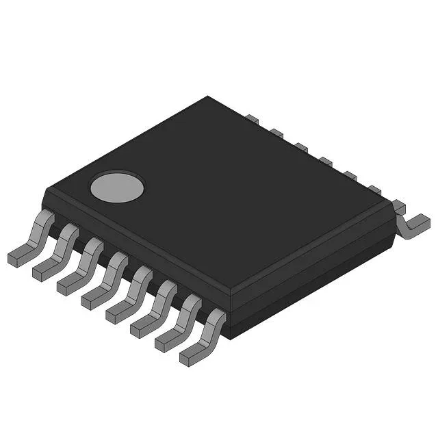
Housed in a 16-pin TSSOP package with a 4.40 mm body width, this part fits a standard surface-mount footprint.
The part is RoHS non-compliant per the ledger — verify your assembly line's solder profile and exemption requirements if you are in a RoHS-regulated jurisdiction.