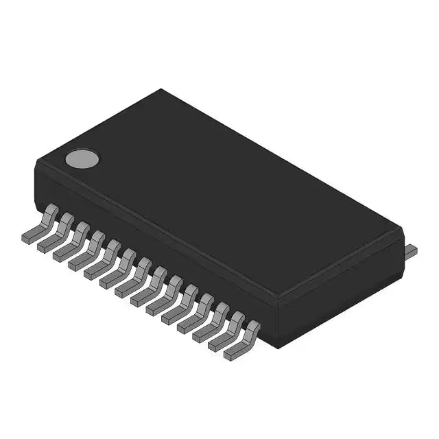
2:12 fanout buffer with on-chip PLL
The CY23FP12OI integrates a phase-locked loop to regenerate a clean clock from a single LVCMOS or LVTTL input and distribute it across twelve LVCMOS outputs — no external PLL components needed on the board. Maximum output frequency is 200 MHz, which covers most DDR, Ethernet, and FPGA reference clock trees without requiring a separate high-speed fanout device.
Supply flexibility and output count
The 2:12 input-to-output ratio is the standout spec: two independent input pins feed twelve outputs, giving a fanout density that a 1:5 part like the CY2305SXI-1HT cannot match without multiple devices. All I/O are single-ended LVCMOS — no differential signalling — so the part is a direct drop-in for legacy or cost-sensitive boards where CML or LVPECL would add BOM cost.
The 28-SSOP package is a standard Infineon footprint, so supply should track mainstream production volumes. RoHS non-compliant — if your assembly line is RoHS-only, factor a waiver or look for a lead-free variant.
Package and footprint checklist
28-SSOP (0.209-inch body width, 5.30 mm height) — surface-mount only. One PLL circuit on die, no divider on the feedback path (multiplier=Yes, divider=No). The zero-delay architecture locks the output edges to the input with near-zero skew — critical for synchronous interfaces where setup/hold margin is tight.