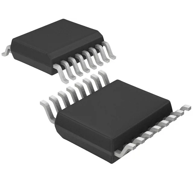
Fanout buffer with PLL bypass for clock distribution
The Cypress CY23EP09ZXI-1H is a fanout buffer and zero-delay buffer that takes one LVCMOS or LVTTL input clock and distributes it to nine LVCMOS outputs. It integrates a PLL with a bypass option, letting you either clean up jitter through the PLL or pass the input clock straight through for low-latency paths. Maximum output frequency reaches 200 MHz (220 MHz on some specs), covering common digital logic, memory interfaces, and FPGA reference clocks.
The dual supply voltage support (2.5V and 3.3V) means it can sit on a 2.5V-core FPGA rail or a 3.3V peripheral bus without a level translator. The 1:9 fanout ratio saves board space by replacing multiple lower-density buffers.
The fine pitch means careful alignment during reflow, but the package is not thermally demanding — no exposed pad to solder.
The ROHS3 compliance covers EU regulatory requirements.