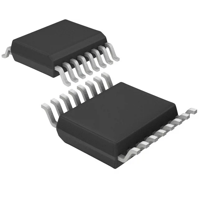
Infineon Technologies CY23EP09ZXC-1H — Clock & Timing ICs

CY23EP09ZXC-1H Zero Delay Buffer, 220 MHz, 16-TSSOP

MPNCY23EP09ZXC-1H
End of Life

Cypress CY23EP09ZXC-1H, Zero Delay Buffer, 1:9 fanout, 220 MHz max, LVCMOS I/O, 2.5V/3.3V supply, 16-TSSOP, 0°C to 70°C.

$18.58Ref. price · indicative, final on quote
Packaging16-TSSOP (0.173", 4.40mm Width)
StockContact for availability
MOQ1 pcs
  • 100% new & originalTraceable channels only — no refurbs, no pulls, no remarked parts.
  • Date & lot codes on quoteStated per line before you commit; label photos on request.
  • MSL-compliant ESD packingMoisture-sealed bags with indicator cards; reels photo-verified.
  • PayPal buyer protectionPay by T/T, PayPal or Payoneer — card payments covered end to end.

Specifications

CY23EP09ZXC-1H Technical Specifications
ParameterValue
TypeFanout Buffer (Distribution), Zero Delay Buffer
Mounting typeSurface Mount
Voltage2.5V, 3.3V
Frequency200MHz, 220MHz
Operating temperature0°C ~ 70°C
PLLYes with Bypass
InputLVCMOS, LVTTL
OutputLVCMOS
PackageTube
Case16-TSSOP (0.173\", 4.40mm Width)
Divider (Multiplier)No/No
Number of circuits1
Ratio - Input:Output1:9
Differential - Input:OutputNo/No

Product details

220 MHz zero-delay buffer with PLL bypass — what that means for your clock tree

The CY23EP09ZXC-1H is a Cypress zero-delay buffer that takes a single LVCMOS or LVTTL input and distributes it to nine LVCMOS outputs with near-zero propagation skew. The internal PLL locks to the input frequency and regenerates the outputs with deterministic phase alignment, which is the defining feature of a zero-delay buffer — the output edges align to the input edge within a few hundred picoseconds, not the propagation delay of a simple fanout gate. The PLL can also be bypassed, letting the device act as a straight fanout buffer when you need the lowest possible additive jitter or want to run at frequencies outside the PLL's lock range. Maximum output frequency is 220 MHz, with a second rating of 200 MHz. Supply voltage is dual-rated at 2.5 V and 3.3 V, so it fits into both legacy 3.3 V clock trees and lower-voltage 2.5 V designs without a separate level translator. The single-circuit, single-ended I/O (no differential inputs or outputs) keeps the pin count and board area down — 16-TSSOP is a compact footprint for a nine-output buffer.

Active lifecycle — no end-of-life risk for this BOM line

For a procurement decision, this means the part is safe to qualify into a new design today — no forced redesign cycle from obsolescence in the near term.

Temperature grade and package — commercial indoor use, surface-mount assembly

Operating temperature range is 0°C to 70°C, the commercial grade. This limits the part to indoor, temperature-controlled environments.

Frequently asked questions

What is the maximum frequency of CY23EP09ZXC-1H?

The CY23EP09ZXC-1H is rated for a maximum output frequency of 220 MHz, with a second rating of 200 MHz. The 220 MHz figure applies when the PLL is bypassed; the 200 MHz rating is for the PLL-locked zero-delay mode. Either way, it covers common clock distribution needs for PCIe, Ethernet, and FPGA reference clocks.