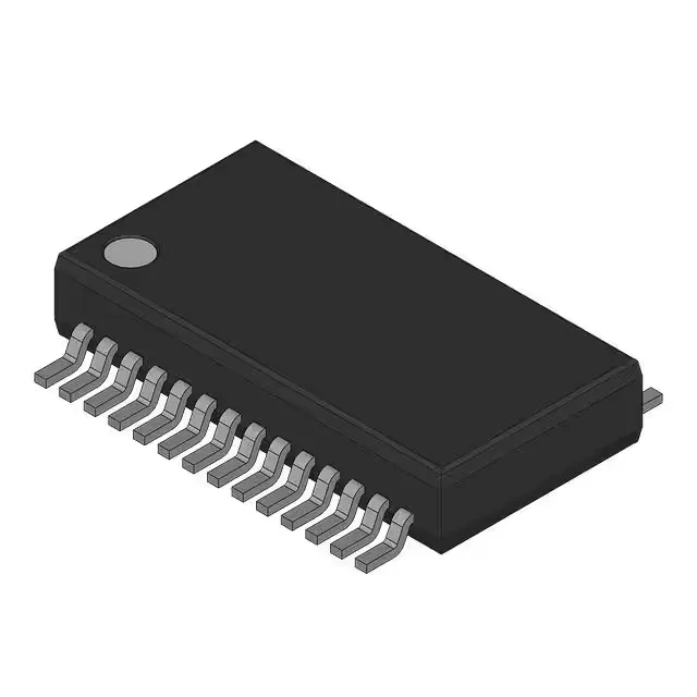
Infineon Technologies CY2310ANZPVC-1 — Analog & Data Acquisition

CY2310ANZPVC-1 Low Skew Clock Driver, 100MHz, 1:10, 28-SSOP

MPNCY2310ANZPVC-1
End of Life

Cypress CY2310ANZPVC-1 low skew clock driver, PLL No, 100MHz max, 1:10 fanout, LVCMOS/LVTTL input, LVCMOS output, 3.135V-3.465V supply, commercial temp 0°C to 70°C, 28-SSOP package.

$5.14Ref. price · indicative, final on quote
Packaging28-SSOP (0.209", 5.30mm Width)
StockContact for availability
MOQ1 pcs
  • 100% new & originalTraceable channels only — no refurbs, no pulls, no remarked parts.
  • Date & lot codes on quoteStated per line before you commit; label photos on request.
  • MSL-compliant ESD packingMoisture-sealed bags with indicator cards; reels photo-verified.
  • PayPal buyer protectionPay by T/T, PayPal or Payoneer — card payments covered end to end.

Specifications

CY2310ANZPVC-1 Technical Specifications
ParameterValue
Mounting typeSurface Mount
Voltage3.135V ~ 3.465V
Frequency100MHz
Operating temperature0°C ~ 70°C (TA)
PLLNo
InputLVCMOS, LVTTL
OutputLVCMOS
PackageBulk
Main purposeIntel CPU, SRAM SO-DIMMs
Case28-SSOP (0.209\", 5.30mm Width)
Number of circuits1
Ratio - Input:Output1:10
Differential - Input:OutputNo/No

Product details

Low skew clock buffer for Intel CPU and SRAM SO-DIMM clock trees

The Cypress CY2310ANZPVC-1 is a low skew clock driver designed to distribute a single reference clock to ten outputs with minimal propagation delay variation. It is a PLL-less buffer, meaning it does not multiply or synthesize frequencies — it simply fans out the input clock with low skew, making it suitable for timing architectures where clock alignment matters more than frequency generation. The part accepts LVCMOS or LVTTL inputs and delivers LVCMOS outputs, operating from a 3.135 V to 3.465 V supply. Its primary application is clock distribution for Intel CPU systems and SRAM SO-DIMM memory modules, where a clean, low-skew copy of the reference clock must reach multiple loads.

1:10 fanout — board-level distribution

With a 1:10 input-to-output ratio, a single reference clock drives up to ten loads. That covers the clock inputs of multiple SRAM chips on a SO-DIMM module, or the CPU and chipset clock inputs on a motherboard. Because the part is a PLL-less buffer, there is no jitter accumulation from a PLL loop — the output jitter is essentially the input jitter plus the buffer's additive jitter, which is typically lower than a PLL-based clock generator. The non-differential I/O (No/No for differential input and output) means it handles single-ended clocks only, not differential pairs like LVDS or HCSL.

Package and temperature grade

The CY2310ANZPVC-1 is offered in a 28-SSOP (5.30 mm body width) surface-mount package, supplier device package 28-SSOP. The operating temperature range is 0°C to 70°C (commercial grade), which limits it to indoor, temperature-controlled environments. It is not rated for automotive, industrial, or extended-temperature applications. The part is RoHS non-compliant (lead-bearing), so verify your assembly house's exemption or plan for a lead-free alternative if required.

Lifecycle and sourcing

The CY2310ANZPVC-1 is listed as Active in production status. The part is (not tape-and-reel), so plan for tube or tray handling in your pick-and-place setup.

Frequently asked questions

What is the CY2310ANZPVC-1's input and output type?

The input accepts LVCMOS or LVTTL levels; the output is LVCMOS. Both are single-ended — no differential I/O is supported.