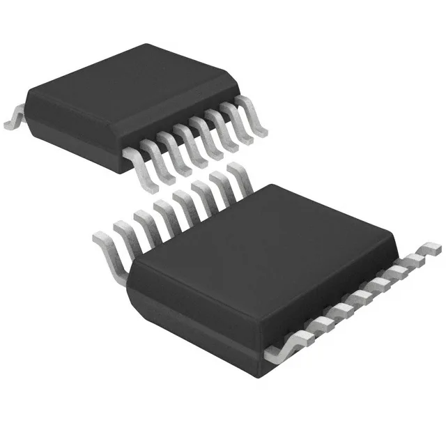
Active zero-delay buffer with 1:9 fanout
The Cypress CY2309ZXI-1H is a zero-delay buffer and fanout distribution IC designed to regenerate and distribute a reference clock to multiple loads with minimal skew. It accepts LVCMOS or LVTTL inputs and outputs LVCMOS signals across nine outputs from a single input, with a PLL that includes a bypass mode for test or low-jitter pass-through operation.
133.33 MHz ceiling and the 1:9 fanout
The 133.33 MHz maximum frequency covers most standard clock distribution needs — PCI Express Gen 1 (100 MHz), Gigabit Ethernet (125 MHz), and common FPGA reference clocks. The 1:9 input-to-output ratio means a single buffer can drive nine loads directly, which simplifies clock-tree layout and reduces the need for multiple fanout stages. The PLL with bypass mode lets you run the clock cleanly through the buffer without phase-locking when the application demands a deterministic path or lower additive jitter.
This is not an automotive-grade part — no AEC-Q100 qualification is listed, so it is not rated for under-hood or chassis-domain environments.
Housed in a 16-TSSOP package (4.40 mm width, 0.173" pitch), surface-mount only. The supplier device package is 16-TSSOP.
No PCN or LTB dates are published for this part number.