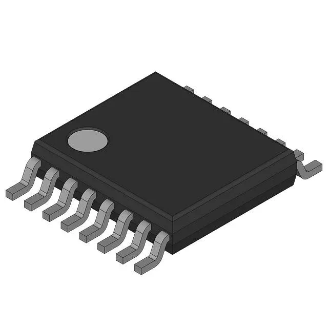
What this PLL clock buffer does on your board
The Cypress CY2309ZC-1HT is a PLL-based Zero Delay Buffer — a clock driver that takes one input clock and regenerates it across nine outputs with minimal phase skew between them. The 'zero delay' label means the device aligns the output edges to the input edge using an internal PLL, so the propagation delay through the buffer is effectively cancelled. It runs from a 3V to 3.6V supply, so it fits comfortably on a 3.3V rail. The input and outputs are single-ended (no differential signalling), which keeps the routing simple on a standard four-layer PCB — no need for controlled-impedance pairs unless your clock rate is high enough to demand them.
1:9 fanout — how many loads it can drive
The 1:9 ratio means one clock input drives nine clock outputs. That is a lot of fanout for a single buffer stage. On a typical board you might see this feeding clock to nine separate DDR memory devices, or distributing a reference clock across a multi-FPGA design. The internal PLL cleans up the input jitter to some degree, but the real win is the low output-to-output skew — the datasheet typical numbers are tight enough that you can run synchronous interfaces without worrying about one load seeing the clock edge earlier than another.
Temperature range — where it can live
It belongs in office equipment, test gear, consumer electronics, or any indoor rack-mounted system. Do not plan to use it in an engine bay, an outdoor base station, or a freezer — the industrial or automotive variants of this family would be the right pick for those environments.
RoHS status — a sourcing gotcha
The CY2309ZC-1HT is marked as RoHS non-compliant.
Cypress lists this part as Active, so it is still being manufactured.
Housed in a 16-TSSOP package with a 4.40mm body width and 0.173-inch pitch. Surface-mount only. The footprint is standard — any PCB layout tool's TSSOP-16 library will match. No exposed pad, so thermal management is straightforward: the part dissipates very little power (it is a clock buffer, not a regulator), so no special via stitching or copper pour is needed under the part.