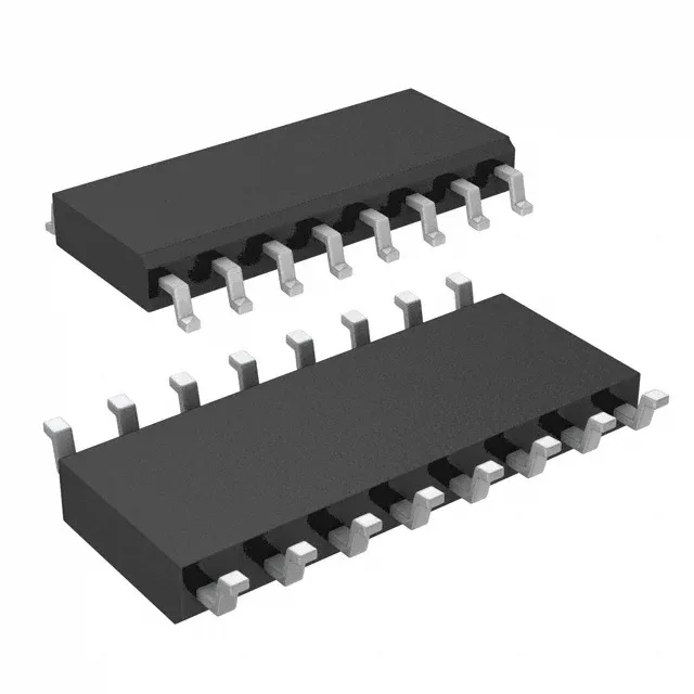
133.33 MHz clock fanout with PLL bypass — what it buys you
The CY2309SXC-1 is a Cypress zero-delay buffer that takes one LVCMOS or LVTTL input and distributes it to nine outputs with matched phase. The on-chip PLL locks the output edges to the input edge, so the propagation delay is effectively zero — useful when you need to fan out a reference clock to multiple loads without skew accumulating across the board. When the PLL is bypassed, the part acts as a straight fanout buffer, passing the input through with its own propagation delay. The max operating frequency is 133.33 MHz, which covers common 100 MHz and 125 MHz reference clocks for Ethernet PHYs, FPGAs, and SoCs. Supply range is 3 V to 3.6 V, so it runs cleanly off a 3.3 V rail.
1:9 ratio vs. the 1:5 sibling
The closest functional peer is the CY2305SXI-1HT, which offers a 1:5 fanout ratio in the same Cypress zero-delay buffer family. Both run at 133.33 MHz max and share the 3.0 V supply rail. The CY2309SXC-1 gives you nine outputs instead of five, saving a second buffer when your clock tree needs to drive six to nine loads. The trade-off is the commercial temperature range (0°C to 70°C) versus the CY2305SXI-1HT's industrial range (-40°C to 85°C). If your ambient stays inside a conditioned room, the CY2309SXC-1 covers the same function at a lower BOM cost per output.