PLL clock buffer with bypass — what it does on your board
The Cypress CY2309ESXC-1H is a PLL-based zero delay buffer that regenerates an incoming clock with near-zero propagation skew across nine outputs. The integrated PLL cleans up jitter and aligns edges; the bypass mode lets you feed the input clock straight through when you want a simple fanout without phase adjustment. It is built for commercial-temperature (0°C to 70°C) equipment — think networking gear, server motherboards, or base-station timing cards where a clean, low-skew clock tree is needed. The 1:9 ratio means one reference clock drives up to nine loads, saving a separate fanout tree and reducing board area.
Supply and temperature — where it fits
Runs on a 3V to 3.6V rail, typical for 3.3V clock distribution in digital systems. If your build sees -40°C, the CY2305SXI-1HT sibling with industrial temp is the alternative to evaluate.
Package and mounting — board fit
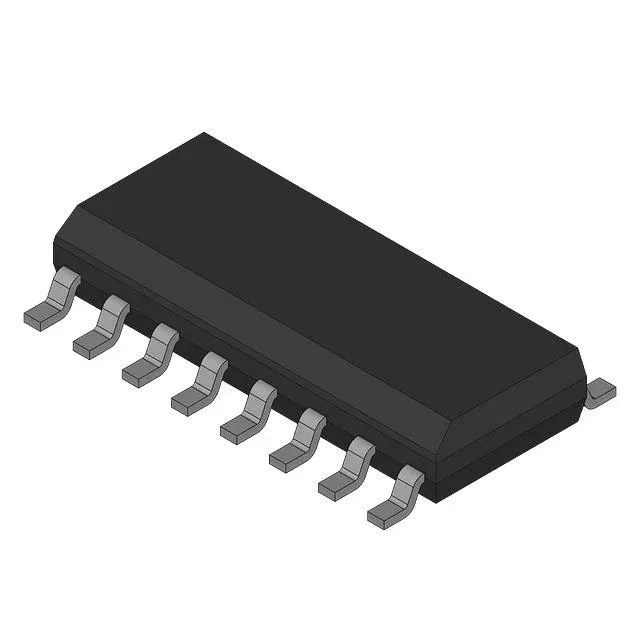
Housed in a 16-SOIC (3.90 mm width) surface-mount package. The 0.154-inch body width is a standard SOIC footprint, so layout is straightforward. No differential signalling on input or output — single-ended CMOS levels only, which simplifies routing but limits noise immunity on long traces.
Marked as Active on the lifecycle record, so no imminent end-of-life or last-time-buy risk for ongoing production. Given the active status, the supply chain is stable for new designs and replacement builds alike.