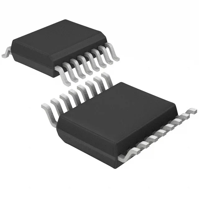
Infineon Technologies CY2309CZXC-1H — Clock & Timing ICs

CY2309CZXC-1H Zero Delay Buffer, 133.33 MHz, 16-TSSOP

MPNCY2309CZXC-1H
End of Life

Cypress CY2309CZXC-1H, Zero Delay Buffer / Fanout Buffer, 1:9 Input:Output, 133.33 MHz max, LVCMOS I/O, 3V-3.6V supply, 0°C to 70°C, 16-TSSOP package.

$1.69Ref. price · indicative, final on quote
Packaging16-TSSOP (0.173", 4.40mm Width)
StockContact for availability
MOQ1 pcs
  • 100% new & originalTraceable channels only — no refurbs, no pulls, no remarked parts.
  • Date & lot codes on quoteStated per line before you commit; label photos on request.
  • MSL-compliant ESD packingMoisture-sealed bags with indicator cards; reels photo-verified.
  • PayPal buyer protectionPay by T/T, PayPal or Payoneer — card payments covered end to end.

Specifications

CY2309CZXC-1H Technical Specifications
ParameterValue
TypeFanout Buffer (Distribution), Zero Delay Buffer
Mounting typeSurface Mount
Voltage3V ~ 3.6V
Frequency133.33MHz
Operating temperature0°C ~ 70°C
PLLYes with Bypass
InputLVCMOS, LVTTL
OutputLVCMOS
PackageTube
Case16-TSSOP (0.173\", 4.40mm Width)
Divider (Multiplier)No/No
Number of circuits1
Ratio - Input:Output1:9
Differential - Input:OutputNo/No

Product details

133.33 MHz zero-delay clock distribution in a 16-TSSOP

The CY2309CZXC-1H is a Cypress zero-delay buffer and fanout buffer that takes one LVCMOS or LVTTL input and distributes it to nine LVCMOS outputs, with a maximum frequency of 133.33 MHz. It integrates a PLL that can be bypassed, letting the part either align output edges to the input for zero-delay operation or pass the clock straight through for test or low-jitter paths. The single 3V to 3.6V supply rail means it drops straight into a 3.3V clock tree without level translation — no extra regulator or level shifter needed on that rail.

1:9 fanout — how many loads it can drive

With a 1:9 input-to-output ratio, a single CY2309CZXC-1H can feed up to nine clock loads — typically FPGA banks, multiple ADCs, or a set of Ethernet PHYs — without needing an external fanout tree. The outputs are non-differential (single-ended LVCMOS), so it is a straightforward drop-in for single-ended clock distribution. If your design needs more than nine copies, you cascade two of these or move to a higher-fanout part.

PLL with bypass — when to use it

The PLL with bypass feature gives you two operating modes. In normal zero-delay mode, the PLL aligns the output edges to the input, compensating for buffer propagation delay so the clock arrives at the loads in phase with the source. In bypass mode, the PLL is shut off and the input passes straight to the outputs — useful for system bring-up, fault isolation, or when the input clock is already clean and you just need fanout without phase alignment. The part has no divider or multiplier, so the output frequency equals the input frequency in both modes.

0°C to 70°C — where this part belongs

The commercial temperature grade (0°C to 70°C) limits this part to indoor, office, or consumer equipment — think network switches, set-top boxes, test equipment in a lab, or appliance control boards. It is not rated for industrial motor drives, outdoor telecom cabinets, or automotive under-hood environments. If your system sees -40°C or +85°C ambient, the sibling CY2305SXI-1HT carries an industrial temperature range but only five outputs.

16-TSSOP — rework and layout notes

The 16-TSSOP package (4.40 mm width, 0.173" pitch) is a fine-pitch surface-mount part that reflows cleanly with a standard lead-free profile. The thermal pad is not exposed, so all heat dissipates through the leads — keep the copper pours under the part generous and use a via stitch to the ground plane if the board runs warm. The part ships in tube, so plan for tube-to-reel transfer if your pick-and-place line expects tape.

Active lifecycle — no LTB risk

ROHS3 compliant per the listing. For a BOM line that needs a zero-delay buffer in a 16-TSSOP, this part is a safe long-term selection without obsolescence-driven redesign risk.

Frequently asked questions

Can CY2309CZXC-1H be used in a 3.3V system without level translation?

Yes. The supply voltage range is 3V to 3.6V, so a 3.3V rail is right in the middle of the operating window. Both the LVCMOS/LVTTL input and LVCMOS outputs are compatible with 3.3V logic levels without any external level shifters.

Can CY2309CZXC-1H be used as a clock generator?

No. This part has no divider or multiplier (Divider/Multiplier: No/No), so the output frequency always equals the input frequency. It is a zero-delay buffer and fanout buffer, not a clock generator. For frequency synthesis you would need a PLL with programmable dividers, such as a dedicated clock generator IC.

Is CY2309CZXC-1H a direct replacement for CY2309CZXC?

The suffix "-1H" indicates a specific speed grade or ordering option. The base part number CY2309CZXC shares the same 16-TSSOP package and 1:9 fanout, but the -1H variant is rated for 133.33 MHz maximum frequency. Without the original CY2309CZXC datasheet in hand, confirm the speed grade matches your requirement before substituting.