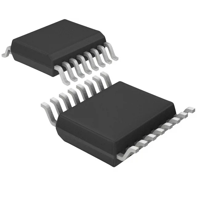
Infineon Technologies CY2308ZXI-1H — Microcontrollers & Processors (MCU / MPU / DSP)

CY2308ZXI-1H Fanout Buffer, 133.3 MHz, 1:8, 16-TSSOP

MPNCY2308ZXI-1H
End of Life

Infineon Technologies Fanout Buffer (Distribution), Zero Delay Buffer, CY2308ZXI-1H, 133.3 MHz max, 1:8 ratio, LVCMOS I/O, 16-TSSOP, -40 to 85°C.

$16.68Ref. price · indicative, final on quote
Packaging16-TSSOP (0.173", 4.40mm Width)
StockContact for availability
Lead timeIn Stock wk
MOQ1 pcs
  • 100% new & originalTraceable channels only — no refurbs, no pulls, no remarked parts.
  • Date & lot codes on quoteStated per line before you commit; label photos on request.
  • MSL-compliant ESD packingMoisture-sealed bags with indicator cards; reels photo-verified.
  • PayPal buyer protectionPay by T/T, PayPal or Payoneer — card payments covered end to end.

Specifications

CY2308ZXI-1H Technical Specifications
ParameterValue
TypeFanout Buffer (Distribution), Zero Delay Buffer
Mounting typeSurface Mount
Voltage3V ~ 3.6V
Frequency133.3MHz
Operating temperature-40°C ~ 85°C
PLLYes with Bypass
InputLVCMOS, LVTTL
OutputLVCMOS
PackageTube
Case16-TSSOP (0.173\", 4.40mm Width)
Divider (Multiplier)No/No
Number of circuits1
Ratio - Input:Output1:8
Differential - Input:OutputNo/No

Product details

133.3 MHz fanout buffer with PLL bypass

The CY2308ZXI-1H is a fanout buffer and zero delay buffer from Infineon Technologies, designed to distribute a single LVCMOS or LVTTL input to eight LVCMOS outputs with minimal skew. The internal PLL can be engaged for zero-delay operation or bypassed for a simple buffer path, giving the board designer flexibility on whether to clean up clock jitter or pass the source through unmodified.

1:8 fanout and frequency ceiling

The 1:8 input-to-output ratio lets one reference clock feed eight loads — for example, distributing a 100 MHz base clock to multiple FPGAs or ASICs on the same board. The maximum output frequency of 133.3 MHz sets the upper limit of the clock tree; anything above that requires a faster part or a different topology. The single-circuit design (one PLL core) means all eight outputs share the same skew characteristics, simplifying timing closure in multi-load synchronous interfaces like DDR memory busses or high-speed serial links where cycle-to-cycle jitter matters.

Active production, ROHS3, and sourcing

Packaged in a 16-TSSOP (4.40 mm width) with surface-mount termination, the part is supplied in tubes. The industrial temperature grade means it can be specified into outdoor or uncontrolled-environment equipment without a derating penalty.

Frequently asked questions

What is the CY2308ZXI-1H's maximum output frequency?

The maximum output frequency is 133.3 MHz. This is the ceiling for the LVCMOS outputs when the PLL is engaged or bypassed.