What the 133.3 MHz ceiling means for your clock tree
The CY2308ZXC-1H is a zero-delay fanout buffer that takes one LVCMOS or LVTTL clock input and distributes it to eight LVCMOS outputs, with a maximum frequency of 133.3 MHz. That ceiling covers most common bus clocks — PCI, Ethernet MAC reference, DDR memory controller interfaces — but not the higher-speed SERDES or RF reference clocks that run above 200 MHz. The integrated PLL has a bypass mode, meaning you can either let the PLL lock and regenerate the output with zero delay relative to the input, or bypass it entirely to pass the input clock through as a simple buffer. This is useful when you need to fan out a clean clock in one part of the board but keep the PLL out of the path for jitter-sensitive sections.
Supply rail and temperature — where it fits
No separate core or I/O voltage needed — one clean 3.3 V plane and a good decoupling cap at each supply pin is the standard layout.
Package and hand-solderability
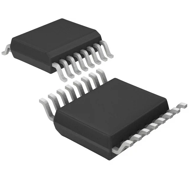
Housed in a 16-TSSOP with 0.65 mm pin pitch and a 4.4 mm body width. The 1:8 ratio means you get eight copies of the input clock from a single 16-pin package, which saves board space compared to daisy-chaining multiple smaller buffers. Each output is LVCMOS, so it drives standard logic inputs directly without external termination resistors for short traces.
Supplied in tube packaging, so it arrives in anti-static tubes suitable for manual assembly or small pick-and-place runs. For reel quantities, check the alternate order code suffix.