Infineon Technologies CY2308ZI-1HT — Clock & Timing ICs

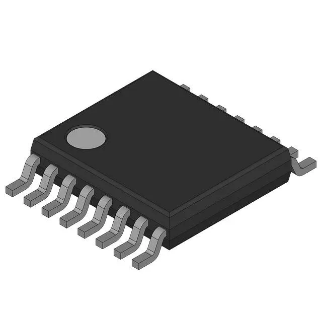
Cypress CY2308ZI-1HT Zero Delay Buffer, 133.3MHz, 16-TSSOP

MPNCY2308ZI-1HT
End of Life

Cypress CY2308ZI-1HT, PLL-based Zero Delay Buffer, 133.3 MHz max frequency, 3V–3.6V supply, 2:4 input:output ratio, 16-TSSOP package, -40°C to 85°C operating temperature.

$3.33Ref. price · indicative, final on quote
Packaging16-TSSOP (0.173", 4.40mm Width)
StockContact for availability
MOQ1 pcs
  • 100% new & originalTraceable channels only — no refurbs, no pulls, no remarked parts.
  • Date & lot codes on quoteStated per line before you commit; label photos on request.
  • MSL-compliant ESD packingMoisture-sealed bags with indicator cards; reels photo-verified.
  • PayPal buyer protectionPay by T/T, PayPal or Payoneer — card payments covered end to end.

Specifications

CY2308ZI-1HT Technical Specifications
ParameterValue
TypeZero Delay Buffer
Mounting typeSurface Mount
Voltage3V ~ 3.6V
Frequency133.3MHz
Operating temperature-40°C ~ 85°C (TA)
PLLYes with Bypass
InputClock
OutputClock
PackageBulk
Case16-TSSOP (0.173\", 4.40mm Width)
Divider (Multiplier)Yes/No
Number of circuits1
Ratio - Input:Output2:4
Differential - Input:OutputNo/No

Product details

PLL-based zero delay buffer for clock distribution

The Cypress CY2308ZI-1HT is a PLL-based zero delay buffer designed to regenerate and fan out a clock signal with low skew. It accepts a single-ended clock input and provides four buffered outputs, with a maximum output frequency of 133.3 MHz. The integrated PLL can be bypassed, allowing the device to function as a simple clock buffer when PLL cleanup is not required. Operating from a 3V to 3.6V supply and rated for -40°C to 85°C, it suits industrial control, telecom line cards, and networking equipment where multiple synchronous clock domains must be derived from one reference.

133.3 MHz ceiling and PLL bypass — what they mean for your design

The 133.3 MHz maximum frequency covers most reference clocks used in Ethernet PHYs, FPGAs, and SoCs. The PLL bypass mode lets you feed a clean external clock straight through without PLL jitter cleanup.

Supply and temperature range

The 3V to 3.6V supply range aligns with standard 3.3V logic rails. The industrial temperature grade (-40°C to 85°C) covers most indoor and outdoor telecom enclosures, but not extended automotive or downhole applications. The 16-TSSOP package (4.40 mm body width) is a common surface-mount footprint; verify the land pattern matches your board's existing clock-buffer layout.

Lifecycle and sourcing

Note that the part is marked RoHS non-compliant, so it is not suitable for lead-free assembly lines unless explicitly exempted.

Frequently asked questions

What is the equivalent or replacement for CY2308ZI-1HT?

The closest functional peer is the CY2305SXI-1HT, also a PLL-based zero delay buffer in a similar package, but with a 1:5 input:output ratio instead of 2:4. The CY2308ZI-1HT offers two input options and four outputs; the CY2305SXI-1HT provides one input and five outputs. Verify pin compatibility before substituting.

Does CY2308ZI-1HT require external components for PLL bypass?

No. The PLL bypass is an internal mode selected via the control pins — no external passive components are needed to enable or disable the PLL.

What is the difference between CY2308ZI-1 and CY2308ZI-1HT?

The suffix -1HT typically indicates a specific tape-and-reel packaging variant or a minor revision. Functionally both are the same PLL-based zero delay buffer with identical specifications. Confirm the exact ordering code with your distributor to ensure correct packaging.