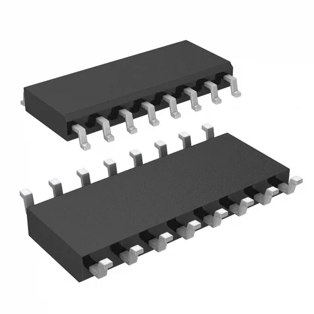
Clock fanout and zero-delay buffer — what the PLL with bypass means for your clock tree
The CY2308SXI-1H is a 1:8 fanout buffer with an integrated PLL that can operate in zero-delay buffer mode — meaning the output edges align in phase with the input reference, not just in frequency. The PLL has a bypass option, so you can feed the reference straight through without phase locking when you need a simple buffer path. Rated for 133.3 MHz maximum output frequency, it takes a single LVCMOS or LVTTL input and replicates it across eight LVCMOS outputs. The single 3V-to-3.6V supply rail keeps the power plane simple.
Industrial temperature grade and what it buys you on the line
The 133.3 MHz ceiling covers most SPI flash, Ethernet PHY, and FPGA reference clock trees — the 1:8 fanout lets one oscillator drive multiple loads without adding a separate clock fanout IC. The PLL with bypass gives you two modes in one footprint: zero-delay buffering for deskewing a multi-drop clock bus, or simple fanout when the PLL is bypassed. That flexibility saves a board spin if the clock topology changes mid-design.