What this buffer does on your clock tree
The Cypress CY2308SXC-1H is a fanout buffer and zero-delay buffer that takes one LVCMOS or LVTTL input and distributes it to eight LVCMOS outputs. It integrates a PLL with bypass mode, so you can either regenerate a clean, phase-aligned copy of the input clock or pass the input straight through when you want the PLL out of the path. Maximum output frequency is 133.3 MHz, which covers most common processor, FPGA, and memory bus clocks in commercial equipment. Supply range is 3V to 3.6V, and the part is specified over 0°C to 70°C — typical for office, telecom indoor, and appliance PCBs.
One input drives eight loads. The 133.3 MHz ceiling is the maximum frequency the outputs can sustain.
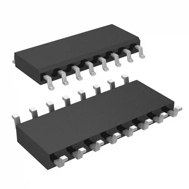
Housed in a 16-pin SOIC with 3.90 mm body width, surface-mount. The 0.154-inch pitch is standard for SOIC-16, so no footprint surprises.
RoHS compliance is standard for the 'XC' suffix; no separate lead-free qualification is needed for EU-market builds.
This is a current-production Cypress (now Infineon) clock buffer. We source it through independent distribution and can quote it against an RFQ.