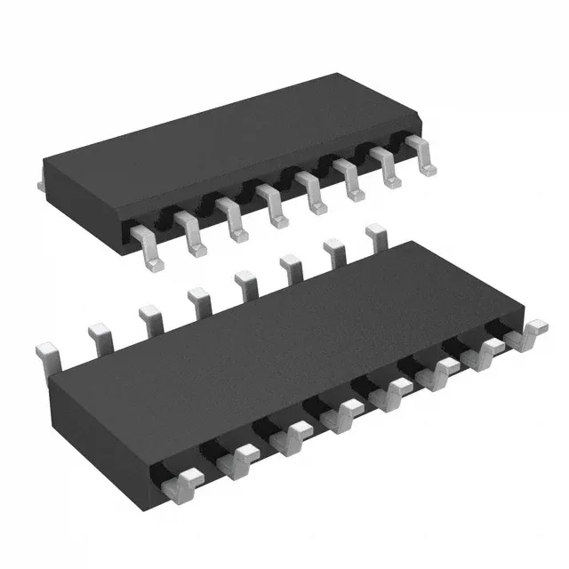
Infineon Technologies CY2308SXC-1 — Discrete Semiconductors

Cypress CY2308SXC-1 Fanout Buffer, 133.3MHz, 1:8, 16-SOIC

MPNCY2308SXC-1
End of Life

Cypress CY2308SXC-1, Fanout Buffer (Distribution), Zero Delay Buffer, 1 circuit, 1:8 input:output, LVCMOS/LVTTL input, LVCMOS output, 133.3MHz max, 3V–3.6V supply, 0°C–70°C, 16-SOIC.

$14.51Ref. price · indicative, final on quote
Packaging16-SOIC (0.154", 3.90mm Width)
StockContact for availability
MOQ1 pcs
  • 100% new & originalTraceable channels only — no refurbs, no pulls, no remarked parts.
  • Date & lot codes on quoteStated per line before you commit; label photos on request.
  • MSL-compliant ESD packingMoisture-sealed bags with indicator cards; reels photo-verified.
  • PayPal buyer protectionPay by T/T, PayPal or Payoneer — card payments covered end to end.

Specifications

CY2308SXC-1 Technical Specifications
ParameterValue
TypeFanout Buffer (Distribution), Zero Delay Buffer
Mounting typeSurface Mount
Voltage3V ~ 3.6V
Frequency133.3MHz
Operating temperature0°C ~ 70°C
PLLYes with Bypass
InputLVCMOS, LVTTL
OutputLVCMOS
PackageTube
Case16-SOIC (0.154\", 3.90mm Width)
Divider (Multiplier)No/No
Number of circuits1
Ratio - Input:Output1:8
Differential - Input:OutputNo/No

Product details

What this clock buffer does on your board

The Cypress CY2308SXC-1 is a fanout buffer and zero delay buffer that takes a single LVCMOS or LVTTL clock input and distributes it to eight LVCMOS outputs with matched edge timing. The internal PLL locks to the input reference and regenerates the outputs so the propagation delay from input to any output is effectively zero — the rising edge at the load aligns with the rising edge at the source. That matters when you are driving multiple clock loads across a PCB and cannot tolerate the cumulative skew of a simple buffer tree. The part runs from a 3V to 3.6V supply, so it drops straight into a 3.3V clock distribution rail. Maximum output frequency is 133.3 MHz, which covers PCI, Ethernet, USB, and most mid-speed processor and FPGA reference clocks. The PLL includes a bypass mode: pull the bypass pin high and the PLL is disabled, the input passes through a delay-matched path to the outputs — useful for test or low-jitter pass-through when you do not need frequency multiplication.

Lifecycle and sourcing posture

The CY2308SXC-1 carries an Active product status and is ROHS3 compliant. There is no NRND flag, no last-time-buy notice, and no announced EOL on this order code. For a BOM line that needs a zero-delay fanout buffer in a 16-SOIC, this part is a current-production choice with no imminent obsolescence risk. No lead-time number is published here, but the part is in active supply and the channel has visibility on multiple date-code lots.

Frequently asked questions

Does CY2308SXC-1 work with 3.3V only, or can it tolerate 2.5V?

The supply range is 3V to 3.6V, so it works on a 3.3V rail but does not tolerate 2.5V. If your clock tree runs at 2.5V, this is not the right buffer.

Is CY2308SXC-1 a direct replacement for CY2308SXC-2?

The evidence does not provide a datasheet comparison between the -1 and -2 suffix variants. Without the -2 spec table, a direct replacement claim cannot be confirmed. Verify the -2 datasheet against the -1's 133.3 MHz max frequency, 1:8 ratio, and 0°C to 70°C temperature range before substituting.

When sourcing CY2308SXC-1, what is the closest functional second-source — CY2305SXI-1HT?

The CY2305SXI-1HT is a 1:5 fanout buffer in the same Cypress family, with the same 133.33 MHz max frequency and PLL architecture, but it is packaged in Tape & Reel and rated for -40°C to 85°C industrial temperature. It is not a pin-for-pin replacement — the output count differs (5 vs 8) and the package may vary. Use it only if your design can accept fewer outputs and the industrial temperature range is acceptable.