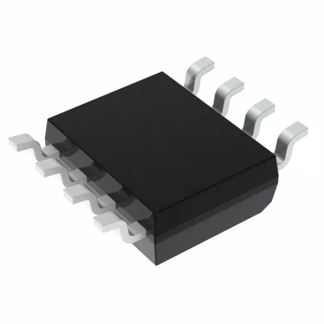
PLL clock distribution in a compact 8-SOIC
The Cypress CY2305SXI-1H is a PLL-based zero-delay buffer that takes one clock input and distributes it to five outputs, each running at the same frequency as the input — no division or multiplication. The internal PLL aligns the output edges to the input, so the propagation delay from input to any output is effectively zero, making it a clean choice for synchronizing multiple clock loads in a system. Maximum output frequency is 133.33 MHz, which covers common 100 MHz and 125 MHz reference clocks used in Ethernet, PCIe, and FPGA designs. The supply range is 3 V to 3.6 V, so it runs comfortably from a 3.3 V rail with typical ±5% tolerance.
What the 1:5 fanout and 133.33 MHz ceiling mean for your design
The 1:5 input-to-output ratio means one reference clock — from an oscillator, crystal, or FPGA output — can feed five downstream devices: multiple Ethernet PHYs, FPGAs, ASICs, or memory controllers. The zero-delay feature keeps the clock edges aligned across all five outputs, which simplifies timing closure in multi-load synchronous designs. The 133.33 MHz maximum is the speed ceiling. The non-differential, single-ended I/O (CMOS) means it's straightforward to route on a PCB but won't reject common-mode noise the way an LVDS or LVPECL buffer would.
Package and mounting — a standard SOIC footprint
The CY2305SXI-1H comes in an 8-pin SOIC package (0.154" body width, 3.90 mm wide), surface-mount only. The footprint is industry-standard and matches countless other 8-SOIC devices, so no special layout considerations are needed. This is a straightforward part for automated pick-and-place and reflow assembly.