PLL clock buffer with 1:9 fanout — what it does on the board
The Cypress CY2305ESXC-1 is a PLL-based zero delay buffer that takes a single clock input and distributes it to nine outputs with near-zero propagation delay between input and output. The internal PLL locks to the incoming clock and regenerates it, cleaning up jitter and providing a low-skew copy to each of the nine outputs. A bypass mode lets the PLL be disabled, passing the input clock straight through — useful for test or low-frequency operation where the PLL's loop filter would otherwise pull the output off frequency. Maximum operating frequency is 133.33 MHz. The 1:9 ratio means one input drives nine loads.
133.33 MHz ceiling — where it fits and where it doesn't
The 133.33 MHz maximum frequency sets a hard upper bound on the clock rate the buffer can pass cleanly. The differential input/output is marked No/No.
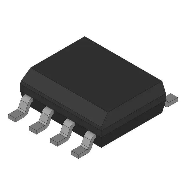
Package and mounting — 8-SOIC, surface mount
Housed in an 8-SOIC package with 0.154" body width and 3.90 mm width, surface-mount only. No through-hole variant exists. The package is small enough for dense layouts but large enough for hand-solder rework if needed.
ROHS3 compliant. For BOM planning, this means no immediate need to qualify a second source, though the CY2305SXI-1HT offers an industrial-temperature variant (-40°C to 85°C) with a 1:5 fanout in the same Cypress family if your thermal environment demands it.