Infineon Technologies CY2304NZZXI-1T — Logic ICs

Cypress CY2304NZZXI-1T Clock Buffer, 140 MHz, 1:4, 8-TSSOP

MPNCY2304NZZXI-1T
End of Life

Cypress CY2304NZZXI-1T zero-delay clock buffer, 1:4 fanout, 140 MHz max, LVCMOS/LVTTL input, LVCMOS output, 3 V to 3.6 V supply, -40°C to 85°C, 8-TSSOP, ROHS3 compliant.

$13.7Ref. price · indicative, final on quote
Packaging8-TSSOP (0.173", 4.40mm Width)
StockContact for availability
MOQ1 pcs
  • 100% new & originalTraceable channels only — no refurbs, no pulls, no remarked parts.
  • Date & lot codes on quoteStated per line before you commit; label photos on request.
  • MSL-compliant ESD packingMoisture-sealed bags with indicator cards; reels photo-verified.
  • PayPal buyer protectionPay by T/T, PayPal or Payoneer — card payments covered end to end.

Specifications

CY2304NZZXI-1T Technical Specifications
ParameterValue
Mounting typeSurface Mount
Voltage3V ~ 3.6V
Frequency140MHz
Operating temperature-40°C ~ 85°C
PLLNo
InputLVCMOS, LVTTL
OutputLVCMOS
PackageTape & Reel (TR); Cut Tape (CT)
Main purposePCI Express (PCIe)
Case8-TSSOP (0.173\", 4.40mm Width)
Number of circuits1
Ratio - Input:Output1:4
Differential - Input:OutputNo/No

Product details

What this clock buffer does on a PCIe board

The Cypress CY2304NZZXI-1T is a zero-delay clock buffer designed for PCI Express reference clock distribution. It takes one LVCMOS or LVTTL input and delivers four identical LVCMOS outputs at up to 140 MHz, with a 1:4 fanout ratio. There is no PLL inside — this is a buffer, not a synthesizer, so the output frequency equals the input frequency with added deterministic delay.

The 140 MHz maximum output frequency covers the 100 MHz reference clock used by PCIe Gen1, Gen2, and Gen3. Gen4 and Gen5 run at higher data rates but still use a 100 MHz reference, so this buffer is fine for those too — the limiting factor is the edge rate and jitter on the output, not the frequency. Because it is a zero-delay buffer (not a PLL), the output tracks the input phase with minimal skew, which simplifies timing closure in a multi-load clock tree.

Package and footprint reality

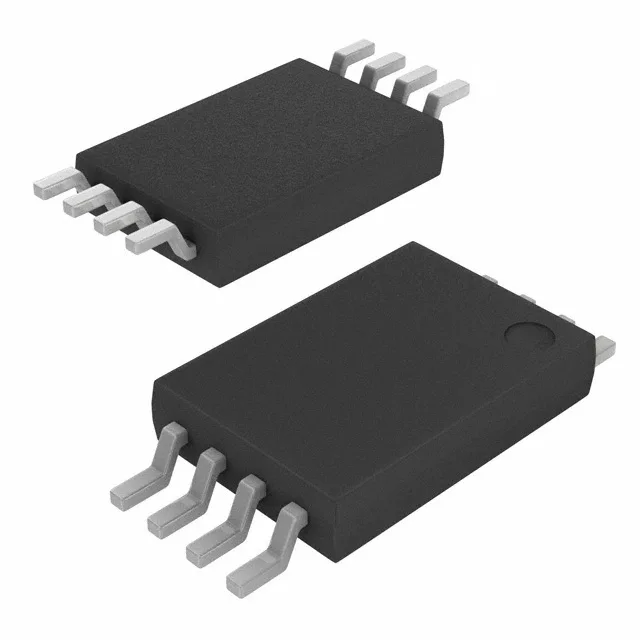
The part comes in an 8-TSSOP package with a 4.40 mm body width — a common, easy-to-route footprint. It is surface-mount only.

Frequently asked questions

Is CY2304NZZXI-1T RoHS compliant?

Yes, the CY2304NZZXI-1T is ROHS3 compliant, meeting the latest EU restriction levels.

What is the difference between CY2304NZZXI-1T and CY2304NZZXI-1?

The -1T suffix indicates Tape & Reel packaging; the -1 suffix (without T) typically ships in tube. The silicon and electrical specifications are identical.

Can CY2304NZZXI-1T be used for PCIe Gen2?

Yes. PCIe Gen2 uses a 100 MHz reference clock, which is well within the 140 MHz maximum frequency of this buffer. The zero-delay architecture provides the low-skew distribution needed for Gen2 timing.