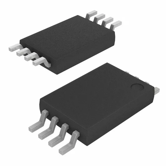
Infineon Technologies CY2304NZZXC-1 — Clock & Timing ICs

CY2304NZZXC-1 Clock Buffer, 140MHz 1:4 PCIe Zero-Delay

MPNCY2304NZZXC-1
End of Life

Cypress CY2304NZZXC-1 clock buffer, zero-delay, 1:4 fanout, 140 MHz max, LVCMOS/LVTTL input, LVCMOS output, 8-TSSOP, 3V-3.6V supply, 0°C to 70°C.

$11.74Ref. price · indicative, final on quote
Packaging8-TSSOP (0.173", 4.40mm Width)
StockContact for availability
MOQ1 pcs
  • 100% new & originalTraceable channels only — no refurbs, no pulls, no remarked parts.
  • Date & lot codes on quoteStated per line before you commit; label photos on request.
  • MSL-compliant ESD packingMoisture-sealed bags with indicator cards; reels photo-verified.
  • PayPal buyer protectionPay by T/T, PayPal or Payoneer — card payments covered end to end.

Specifications

CY2304NZZXC-1 Technical Specifications
ParameterValue
Mounting typeSurface Mount
Voltage3V ~ 3.6V
Frequency140MHz
Operating temperature0°C ~ 70°C
PLLNo
InputLVCMOS, LVTTL
OutputLVCMOS
PackageTube
Main purposePCI Express (PCIe)
Case8-TSSOP (0.173\", 4.40mm Width)
Number of circuits1
Ratio - Input:Output1:4
Differential - Input:OutputNo/No

Product details

PCIe clock distribution in an 8-pin TSSOP

The CY2304NZZXC-1 is a 1:4 zero-delay clock buffer from Infineon (formerly Cypress) designed specifically for PCI Express (PCIe) reference clock distribution. It accepts a single LVCMOS or LVTTL input and delivers four LVCMOS outputs at up to 140 MHz, with no PLL on chip — meaning it's a straight-through fanout buffer, not a jitter cleaner or frequency synthesizer. The 8-TSSOP package (0.173" body width) keeps the footprint small for tight layout zones on a motherboard or add-in card.

140 MHz ceiling — what it means for PCIe generation fit

The 140 MHz maximum output frequency aligns with PCIe Gen 1 and Gen 2 reference clock requirements (100 MHz nominal, spread-spectrum capable). For Gen 3 and Gen 4, the reference clock typically runs at 100 MHz as well, but the jitter and phase-noise specs tighten considerably — this buffer has no PLL to clean up incoming jitter, so the upstream clock source quality determines whether the system meets the Gen 3/4 jitter budget. If your design targets Gen 1 or Gen 2, this part is a clean fit; for Gen 3 or later, verify the total jitter contribution against the PCIe base spec with your specific reference oscillator.

Single-ended I/O only — no differential support

Both the input and output are single-ended (LVCMOS/LVTTL in, LVCMOS out), with no differential signaling on either side. This means the CY2304NZZXC-1 cannot directly buffer a differential HCSL or LVDS PCIe clock — it expects a single-ended reference. If your clock source is differential, you will need a differential-to-single-ended converter ahead of this buffer, or choose a part with differential I/O. For systems already running a single-ended 100 MHz reference from a crystal oscillator or clock generator, this is a straightforward drop-in.

0°C to 70°C — commercial temperature grade

The operating temperature range is 0°C to 70°C, which covers standard commercial and office-environment equipment. This part is not rated for industrial (-40°C to 85°C) or automotive environments — if your system sees outdoor, under-hood, or factory-floor temperatures, look for an industrial-grade variant in the same family. For desktop PCs, servers in climate-controlled data centers, or telecom equipment in conditioned bays, the commercial range is adequate.

Supply rail and package

Operates from a single 3.3 V supply (3 V to 3.6 V range), which is the standard PCIe reference clock voltage. The 8-TSSOP package with 0.173" body width and 4.40 mm width is a common footprint; the supplier device package is also 8-TSSOP. Surface-mount only, no through-hole option. ROHS3 compliant per the lifecycle record.

Active lifecycle — no end-of-life concern

For a BOM line that needs a stable PCIe clock buffer without obsolescence risk over the next several years, this part is a safe choice for new designs.

Frequently asked questions

Can CY2304NZZXC-1 be used for PCIe Gen 2 or Gen 3?

The 140 MHz maximum frequency covers the 100 MHz reference clock used by PCIe Gen 1, Gen 2, and Gen 3. However, this is a zero-delay buffer with no PLL, so it does not clean jitter. For Gen 1 and Gen 2, the jitter budget is typically met with a clean reference oscillator. For Gen 3, the tighter jitter requirements mean you must verify the total system jitter — including this buffer — against the PCIe base specification.

What is the difference between CY2304NZZXC-1 and CY2304NZZXC-1T?

The CY2304NZZXC-1 and CY2304NZZXC-1T share the same electrical specifications — 1:4 fanout, 140 MHz max, LVCMOS I/O, same package. The suffix difference typically indicates tape-and-reel packaging for the -1T variant versus tube for the -1. Pin-compatible and functionally identical; the choice is a logistics preference for your assembly line's feeder setup.

What is the difference between CY2304NZZXC-1 and CY2304NZZXC-2?

The CY2304NZZXC-1 and CY2304NZZXC-2 are both 1:4 zero-delay buffers in the same family, but the -2 variant typically offers a higher maximum frequency or different output drive strength. Without the -2 datasheet in hand, the safest assumption is that the -1 is the 140 MHz baseline part. If you need a higher speed grade, check the -2 specification against your timing budget.

Is CY2304NZZXC-1 RoHS compliant?

Yes, the CY2304NZZXC-1 is ROHS3 Compliant per the lifecycle record.