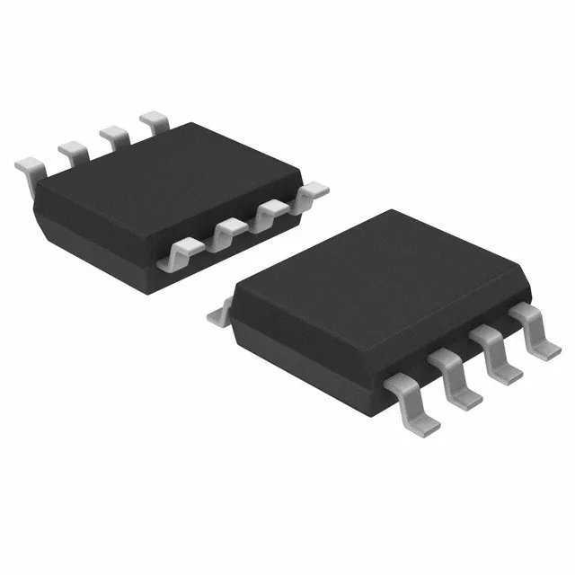
PLL clock multiplier with 166.67 MHz ceiling
The CY2303SXC integrates a phase-locked loop (PLL) to multiply an input reference clock (LVCMOS or LVTTL) and distribute it to three LVCMOS outputs, with a maximum output frequency of 166.67 MHz. The 1:3 fanout ratio lets a single reference clock feed three downstream loads — common in FPGA, SoC, or memory-controller clock trees where a clean multiplied clock is needed without adding a separate oscillator per load.
The supply range (3V to 3.6V) centres on 3.3V, matching the standard I/O voltage for most mid-range FPGAs and SoCs. The 3V lower edge allows operation on a slightly droopy rail, but don't expect full performance below 3.0V. Differential inputs and outputs are not supported (: No/No) — all I/O are single-ended LVCMOS, which simplifies PCB routing but limits noise immunity on long traces compared to a differential pair.
Active production, ROHS3, 8-SOIC package
For industrial or automotive use, an industrial-temperature suffix (e.g., CY2303SXI) would be required.