Fanout and frequency — sizing the clock tree
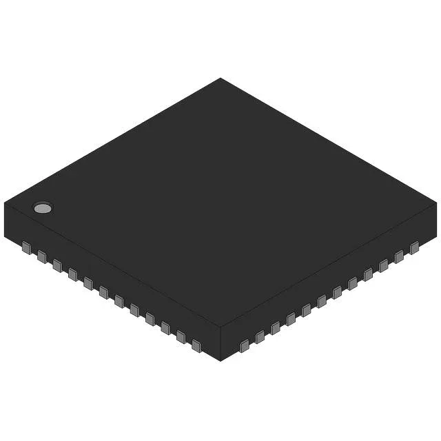
With a 2:21 input-to-output ratio and a maximum output frequency of 200 MHz, this buffer can drive twenty-one loads from one or two reference clocks. That's enough fanout for a mid-size FPGA bank or a handful of SERDES transceivers. The non-differential I/O (No/No) means it's intended for single-ended LVCMOS distribution, not differential pairs like LVPECL or CML. If your design needs differential clocking, this isn't the part.
RoHS non-compliant.