What this clock generator does and who specifies it
The CY22381FXI is a single-circuit PLL clock generator with fanout distribution — it takes a low-frequency LVTTL or crystal input and synthesizes up to three CMOS outputs at frequencies up to 166 MHz. The PLL includes a bypass mode, which lets you feed the input straight through for test or low-jitter paths without reconfiguring the board. Design engineers reach for this part when they need a clean, programmable clock from a simple crystal on a 3.3V rail and want to distribute it to three loads without adding a separate fanout buffer. The industrial temperature range means it can live in a motor drive or outdoor telecom enclosure without a commercial-grade workaround.
The 166 MHz ceiling covers most MCU, FPGA, and Ethernet PHY reference clocks. The 1:3 input-to-output ratio means one crystal feeds three clock loads. Supply voltage tolerance is 3.135V to 3.465V — a 3.3V rail with ±5% regulation. If your board's 3.3V bus droops below 3.135V under load, the PLL may lose lock and the output frequency drifts. Budget a regulator with tight line/load regulation for this rail. The PLL bypass mode is useful during board bring-up: you can feed a known-good reference clock directly to the outputs and isolate the PLL as a variable. No differential I/O — all signals are single-ended CMOS, which keeps the layout simple but limits noise immunity on long traces.
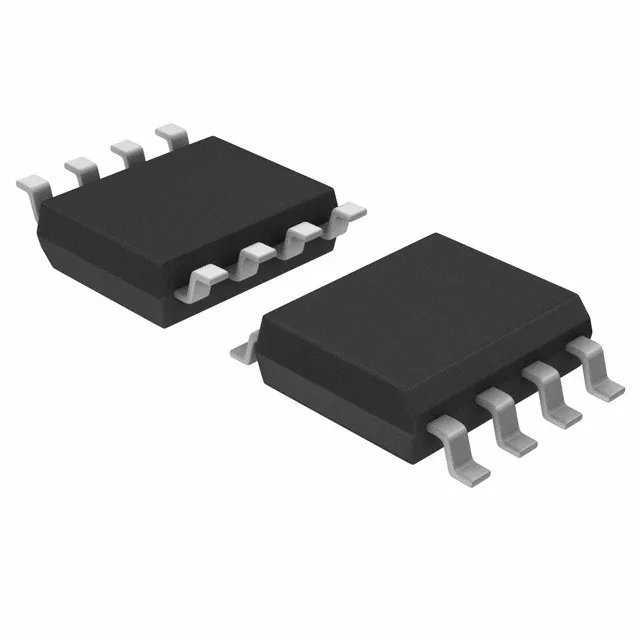
The 8-SOIC package (0.154-inch width, 3.90 mm body) is a standard footprint — no fine-pitch alignment, no hidden thermal pad. Rework is straightforward with a hot-air pencil; no moisture-bake required for typical floor life.