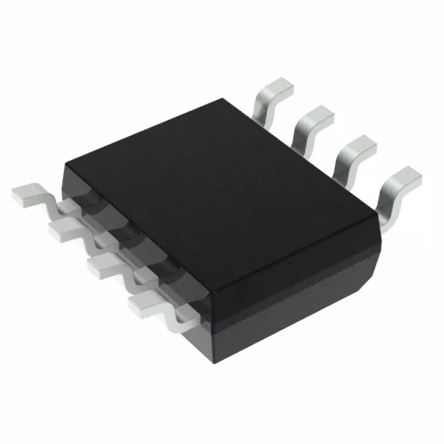
Where this FRAM fits on the board
The CY15B128Q-SXA is a 128Kbit non-volatile FRAM with an SPI interface, clocked at 40 MHz. It stores configuration parameters, calibration constants, or data-log buffers in a system that cannot tolerate the write-cycle wear of EEPROM or the erase-before-write latency of flash. The 8-pin SOIC footprint drops straight onto a 0.154-inch-wide body with 1.27 mm pitch, a common layout for MCU companion memory.
FRAM behaviour that changes the firmware design
Unlike EEPROM or NOR flash, FRAM writes at bus speed with no write-cycle penalty — the 40 MHz SPI clock is the only speed limit. There is no page buffer to manage, no sector-erase command, and no wear-leveling algorithm in the driver. A firmware engineer can treat this memory like a byte-addressable SRAM that happens to retain data after power loss.
Lifecycle and sourcing posture
The part is marked RoHS non-compliant per the manufacturer's declaration. For designs requiring RoHS compliance, the buyer should verify the specific date-code or request the RoHS-compliant variant from Infineon's F-RAM family.