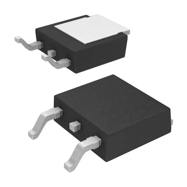
The 46 mOhm typical Rds(on) at 25°C sets the conduction loss at 0.6 W at the 3.6 A maximum continuous output current — a figure that doubles at 150°C junction temperature as the silicon warms, so the thermal budget in the TO-252-3 (DPak) package needs the copper pad area on the PCB to keep the junction below the 150°C absolute maximum.
Integrated fault protection — no external clamp diodes needed
The switch integrates fixed current limiting, over-temperature shutdown, and over-voltage protection, so the BOM does not need a separate TVS or current-sense resistor for basic fault coverage. The input is non-inverting with a 1:1 ratio — logic high turns the output on — and the supply voltage (Vcc) is not required because the gate drive is self-supplied from the load voltage.
60 V load voltage — headroom for automotive load-dump
Rated for a 60 V maximum load voltage, the BTS3046SDLATMA1 handles the 12 V and 24 V battery rails with margin for load-dump transients that can reach 40 V in 12 V systems and 60 V in 24 V systems.
TO-252-3 package — thermal pad layout matters
The PG-TO252-3-11 (DPak, 2 leads plus tab) package requires a copper pad on the PCB under the exposed tab to dissipate heat. The tab is the drain terminal, so the pad is at load voltage. For a 3.6 A load with 46 mOhm Rds(on) at 25°C, the I²R loss is 0.6 W; at 150°C junction the Rds(on) roughly doubles, pushing the loss to 1.2 W. A 1-inch-square copper pad on a 2-layer board keeps the junction temperature rise under 50°C in still air.