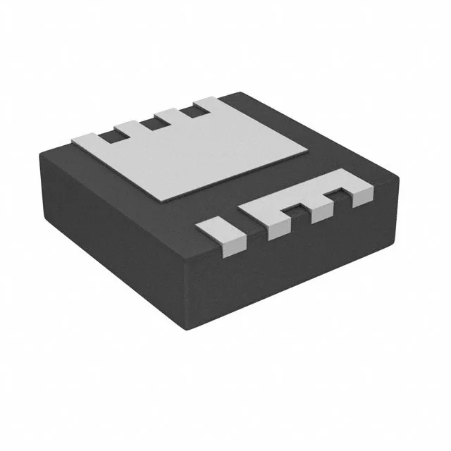
The BSZ300N15NS5ATMA1: It comes in a PG-TSDSON-8-FL package — a 5 mm × 6 mm footprint with an exposed drain pad for thermal management. The 150 V Vdss puts it squarely in the 48 V and 72 V bus applications: telecom rectifiers, battery-management systems, e-bike motor drives, and industrial auxiliary power supplies.
Gate drive and switching — sizing the driver to the gate charge
That means the gate-drive rail must deliver at least 8 V to turn the FET fully on; a standard 12 V gate-drive supply is fine, but a 5 V logic-level drive will not saturate this part to its rated Rds(on). An engineer sizing the gate-drive resistor should plan for a peak gate current that charges 13 nC within the target switching period.
Thermal design — junction temperature and power dissipation
The input capacitance is 950 pF at 75 V Vds, which is moderate and does not demand an aggressive pre-drive stage.
ROHS3 compliant. No official second-source cross-reference is listed, but the IPD50R950CEAUMA1 (CoolMOS CE, 500 V, 950 mOhm) is a different voltage and Rds(on) class — it is not a functional substitute for this 150 V / 30 mOhm part.