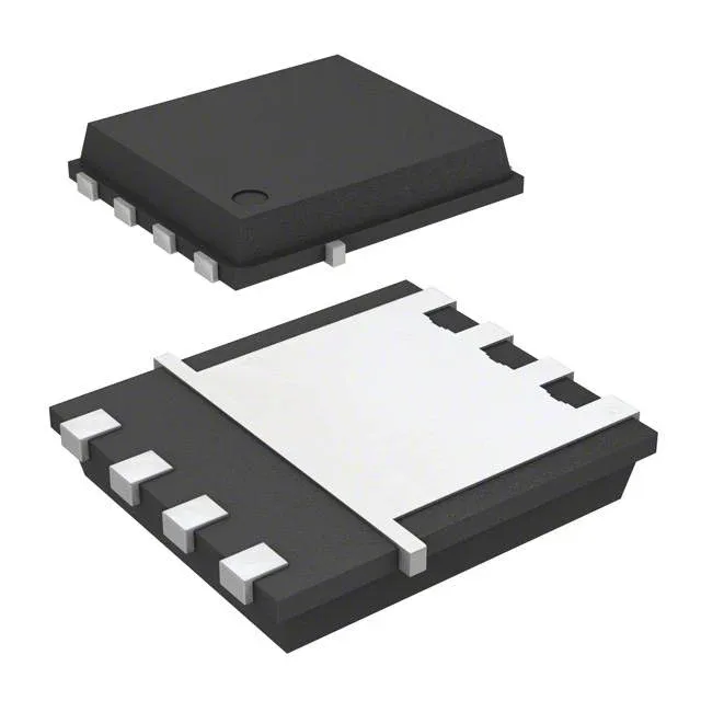
Infineon Technologies BSZ180P03NS3GATMA1

Infineon BSZ180P03NS3GATMA1 P-Channel MOSFET, 30 V, 18 mOhm

MPNBSZ180P03NS3GATMA1
End of Life

Infineon OptiMOS™ BSZ180P03NS3GATMA1, P-Channel MOSFET, 30 V Vdss, 18 mOhm Rds(on) @ 20 A, 10 V, 9 A (Ta) / 39.6 A (Tc), PG-TSDSON-8, -55°C to 150°C.

$0.79Ref. price · indicative, final on quote
Packaging8-PowerTDFN
StockContact for availability
MOQ1 pcs
  • 100% new & originalTraceable channels only — no refurbs, no pulls, no remarked parts.
  • Date & lot codes on quoteStated per line before you commit; label photos on request.
  • MSL-compliant ESD packingMoisture-sealed bags with indicator cards; reels photo-verified.
  • PayPal buyer protectionPay by T/T, PayPal or Payoneer — card payments covered end to end.

Specifications

BSZ180P03NS3GATMA1 Technical Specifications
ParameterValue
SeriesOptiMOS™
FET typeP-Channel
Mounting typeSurface Mount
Drain to source voltage30 V
Drive voltage (Max rds on, min rds on)6V, 10V
Current - continuous drain (Id) @ 25°C9A (Ta), 39.6A (Tc)
Power dissipation2.1W (Ta), 40W (Tc)
Operating temperature-55°C ~ 150°C (TJ)
PackageTape & Reel (TR); Cut Tape (CT)
Vgs±25V
TechnologyMOSFET (Metal Oxide)
Case8-PowerTDFN
Vgs(th) (Max) @ id3.1V @ 48µA
Rds on (Max) @ id, vgs18mOhm @ 20A, 10V
Gate charge (Qg) (Max) @ vgs30 nC @ 10 V
Input capacitance (Ciss) (Max) @ vds2220 pF @ 15 V

Product details

P-channel switch for load and OR-ing applications

The Infineon BSZ180P03NS3GATMA1 is a 30 V P-Channel MOSFET from the OptiMOS™ series, built on a metal-oxide trench technology. It delivers a maximum continuous drain current of 9 A at 25°C ambient (Ta) and 39.6 A when the case is held at 25°C (Tc), with an on-resistance of 18 mOhm max at a 20 A drain current and 10 V gate drive. The part is housed in a PG-TSDSON-8 package (8-PowerTDFN) and operates across a junction temperature range of -55°C to 150°C, making it suitable for automotive under-hood and industrial environments where ambient temperatures can spike.

Package and footprint

The PG-TSDSON-8 is a surface-mount PowerTDFN with an exposed thermal pad. The pad must be soldered to a copper plane on the PCB to achieve the 39.6 A case-rated current and 40 W power dissipation. The 2220 pF input capacitance at 15 V drain-source is typical for a 30 V P-channel in this package class; the gate driver should be placed close to the FET to minimize loop inductance.

Lifecycle and sourcing

The BSZ180P03NS3GATMA1 is listed as Active in production with ROHS3 compliance. No NRND or EOL notices are on record. There is no pin-compatible second source in the OptiMOS P-channel portfolio at this voltage and Rds(on) tier; the N-channel CoolMOS™ IPD50R950CEAUMA1 is a different polarity and voltage class (500 V N-Channel) and is not a functional substitute.

Frequently asked questions

What is the Rds(on) of BSZ180P03NS3GATMA1 at typical operating conditions?

The maximum Rds(on) is 18 mOhm at a drain current of 20 A with a 10 V gate drive. At 6 V gate drive the on-resistance will be higher — the datasheet specifies the drive voltage range for max and min Rds(on) as 6 V and 10 V respectively.

What package is BSZ180P03NS3GATMA1 and what is the footprint?

The BSZ180P03NS3GATMA1 is housed in a PG-TSDSON-8 package, which is an 8-lead PowerTDFN with an exposed thermal pad. The supplier device package is PG-TSDSON-8; the general package / case is 8-PowerTDFN.

Is there a replacement or equivalent for BSZ180P03NS3GATMA1?

No direct pin-compatible second source is listed in the OptiMOS P-channel family at this voltage and Rds(on) tier. The N-channel IPD50R950CEAUMA1 is a different polarity and 500 V class — not a functional substitute. For dual-sourcing options, review the Infineon OptiMOS P-channel 30 V portfolio for parts with similar Rds(on) and package.