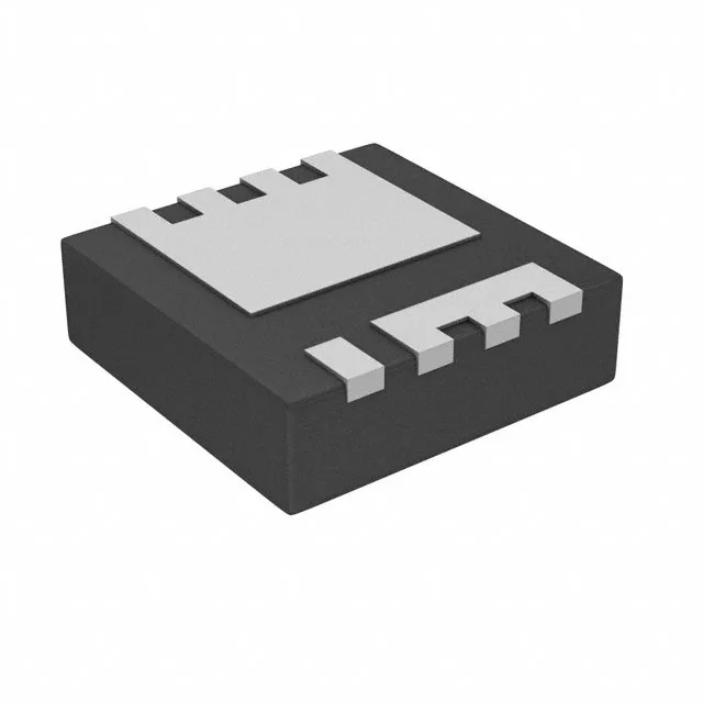
BSZ100N06NSATMA1

Infineon Technologies · OptiMOS™ Series

Infineon OptiMOS™ BSZ100N06NSATMA1, N-Channel MOSFET, 60 V Vdss, 40 A continuous drain, 10 mOhm Rds(on) at 20 A, 10 V gate drive, 15 nC gate charge, 1075 pF input capacitance, PG-TSDSON-8-FL package, -55 to 150 °C junction temperature.

Infineon Technologies BSZ100N06NSATMA1
Download datasheet (PDF)
[IN STOCK] In Stock: 30 pcs
$1.49/ pc

Volume pricing

Buy Now

MOQ 1 · Tape & Reel (TR); Cut Tape (CT) · RoHS · EIA-481 · DAP/DDP · T/T

Technical specifications

BSZ100N06NSATMA1 specifications
Parameter / AttributeSpecification / Value
SeriesOptiMOS™
FET typeN-Channel
MountingSurface Mount
Drain to source voltage60 V
Drive voltage (Max rds on, min rds on)6V, 10V
Current - continuous drain (Id) @ 25°C40A (Tc)
Power dissipation2.1W (Ta), 36W (Tc)
Operating temperature-55°C ~ 150°C (TJ)
PackageTape & Reel (TR); Cut Tape (CT)
Vgs±20V
TechnologyMOSFET (Metal Oxide)
Case8-PowerTDFN
Vgs(th) (Max) @ id3.3V @ 14µA
Rds on (Max) @ id, vgs10mOhm @ 20A, 10V
Gate charge (Qg) (Max) @ vgs15 nC @ 10 V
Input capacitance (Ciss) (Max) @ vds1075 pF @ 30 V

Technical details

10 mOhm Rds(on) — the number that drives the thermal design

At 25 °C junction, a 20 A load dissipates 4 W — well within the 36 W case-rated power dissipation. The actual Rds(on) rises with junction temperature; at 150 °C the on-resistance roughly doubles, so the 4 W loss at 20 A becomes 8 W. The thermal budget must account for this increase. The gate threshold voltage maximum is 3.3 V at 14 µA drain current. The drive voltage range for minimum Rds(on) is 6 V to 10 V.

Gate charge and switching — 15 nC at 10 V

The input capacitance is 1075 pF at 30 V Vds.

Package and thermal path — PG-TSDSON-8-FL

The junction-to-ambient thermal resistance is 2.1 W per °C (Ta) and 36 W per °C (Tc).

BSZ100N06NSATMA1
[ALLOC] verified
Quote