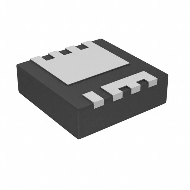
Infineon Technologies BSZ070N08LS5ATMA1

Infineon BSZ070N08LS5ATMA1 N-Channel MOSFET, 80 V, 40 A

MPNBSZ070N08LS5ATMA1
End of Life

Infineon OptiMOS™ 5 N-channel MOSFET, BSZ070N08LS5ATMA1, 80 V Vdss, 40 A Id, 7 mOhm Rds(on) at 10 V, PG-TSDSON-8-FL surface-mount package.

$1.58Ref. price · indicative, final on quote
Packaging8-PowerTDFN
StockContact for availability
MOQ1 pcs
  • 100% new & originalTraceable channels only — no refurbs, no pulls, no remarked parts.
  • Date & lot codes on quoteStated per line before you commit; label photos on request.
  • MSL-compliant ESD packingMoisture-sealed bags with indicator cards; reels photo-verified.
  • PayPal buyer protectionPay by T/T, PayPal or Payoneer — card payments covered end to end.

Specifications

BSZ070N08LS5ATMA1 Technical Specifications
ParameterValue
SeriesOptiMOS™ 5
FET typeN-Channel
Mounting typeSurface Mount
Drain to source voltage80 V
Drive voltage (Max rds on, min rds on)4.5V, 10V
Current - continuous drain (Id) @ 25°C40A (Tc)
Power dissipation69W (Tc)
Operating temperature-55°C ~ 150°C (TJ)
PackageTape & Reel (TR); Cut Tape (CT)
Vgs±20V
TechnologyMOSFET (Metal Oxide)
FET featureStandard
Case8-PowerTDFN
Vgs(th) (Max) @ id2.3V @ 36µA
Rds on (Max) @ id, vgs7mOhm @ 20A, 10V
Gate charge (Qg) (Max) @ vgs5 nC @ 4.5 V
Input capacitance (Ciss) (Max) @ vds2340 pF @ 40 V

Product details

80 V N-channel for 48 V rails and high-density switching

The BSZ070N08LS5ATMA1 from Infineon's OptiMOS™ 5 family is an N-channel enhancement-mode MOSFET rated at 80 V drain-source and 40 A continuous drain current.

7 mOhm Rds(on) — what it means for conduction loss

At 40 A full load, the conduction loss (I² × R) lands around 11.2 W at 25°C junction — well within the 69 W package dissipation capability, but real junction temperature rise will increase Rds(on) by roughly 50% at 125°C, so the loss budget needs a derating factor. The drive voltage range (4.5 V to 10 V) means a standard 5 V or 10 V gate driver can fully enhance the channel; using 4.5 V logic-level drive raises Rds(on) slightly but still achieves useful on-resistance for lower-current branches.

Gate charge and switching speed

Total gate charge is 5 nC at 4.5 V and 2340 pF input capacitance at 40 V drain bias — a light capacitive load that lets the MOSFET switch fast without a high-current gate driver.

Package and thermal path

Housed in an 8-PowerTDFN (PG-TSDSON-8-FL), this package exposes the large drain pad on the bottom — the primary heat path is through the pad into the PCB copper plane. The 69 W power dissipation rating assumes the pad is soldered to a thermal land with adequate via array to inner layers. Without that, the effective RthJA rises and the 40 A continuous rating derates. The package is surface-mount, compatible with standard reflow profiles for lead-free solder.

Temperature range and operating environment

The 150°C absolute maximum junction means the part can survive short-duration overtemperature events, but continuous operation above 125°C should be verified against the thermal derating curve for Rds(on) and leakage.

Lifecycle and sourcing posture

It is ROHS3 compliant.

Frequently asked questions

What are the specifications of BSZ070N08LS5ATMA1?

Engineers need exact specs like Vdss, Rds on, and gate charge to validate fit.

Where can I buy BSZ070N08LS5ATMA1?

Buyers need to source the part quickly from reliable distributors.

What is the price of BSZ070N08LS5ATMA1?

Sourcing buyers compare costs to stay within budget.

Is BSZ070N08LS5ATMA1 obsolete or still active?

Lifecycle status affects long-term availability and design viability.

What is the equivalent or replacement for BSZ070N08LS5ATMA1?

Engineers and buyers need cross-reference options for second sourcing or obsolescence.

What is the pinout and package of BSZ070N08LS5ATMA1?

Design engineers need pinout for PCB layout and footprint compatibility.