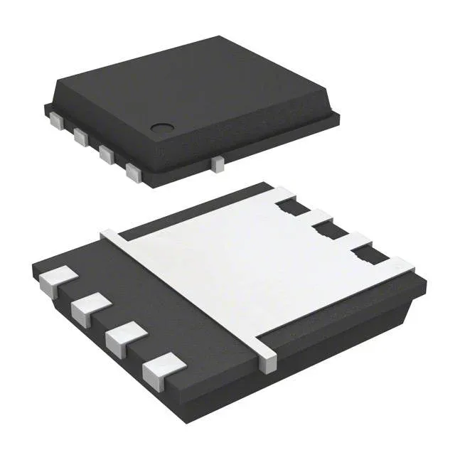
Infineon Technologies BSZ035N03MSGATMA1

Infineon BSZ035N03MSGATMA1 OptiMOS N-Ch 30V 40A MOSFET

MPNBSZ035N03MSGATMA1
End of Life

Infineon OptiMOS™ BSZ035N03MSGATMA1, N-Channel MOSFET, 30V Vdss, 3.5mOhm Rds(on) at 20A, 10V, 40A continuous drain (Tc), PG-TSDSON-8 package, -55°C to 150°C.

$1.18Ref. price · indicative, final on quote
Packaging8-PowerTDFN
RoHSROHS3 Compliant
SeriesOptiMOS™
Independent supplier — new & surplus stockAuthenticity-screened · ESD-safe packingListing updated Jul 2026

Specifications

BSZ035N03MSGATMA1 specifications
ParameterValue
SeriesOptiMOS™
FET typeN-Channel
MountingSurface Mount
Drain to source voltage30 V
Drive voltage (Max rds on, min rds on)4.5V, 10V
Current - continuous drain (Id) @ 25°C18A (Ta), 40A (Tc)
Power dissipation2.1W (Ta), 69W (Tc)
Operating temperature-55°C ~ 150°C (TJ)
PackageTape & Reel (TR); Cut Tape (CT)
Vgs±20V
TechnologyMOSFET (Metal Oxide)
Case8-PowerTDFN
Vgs(th) (Max) @ id2V @ 250µA
Rds on (Max) @ id, vgs3.5mOhm @ 20A, 10V
Gate charge (Qg) (Max) @ vgs74 nC @ 10 V
Input capacitance (Ciss) (Max) @ vds5700 pF @ 15 V

Product details

3.5 mOhm at 10V — the on-resistance that decides the thermal budget

The BSZ035N03MSGATMA1 is an Infineon OptiMOS N-channel MOSFET rated for 30V drain-source and 40A continuous drain at the case (Tc), with a maximum on-resistance of 3.5 mOhm at 20A and 10V gate drive. That Rds(on) figure is the spec that sets the conduction loss floor for a 12V or 24V rail switch — at 20A the dissipation is just 1.4W in the channel, before package thermal resistance enters the calculation.

18A at ambient vs 40A at case — reading the dual current rating

The datasheet lists 18A continuous drain at 25°C ambient (Ta) and 40A at the case (Tc). That 2.2x spread tells you the PG-TSDSON-8 package's thermal limit, not the silicon — the 2.1W (Ta) vs 69W (Tc) power dissipation figures confirm the package is the bottleneck for board-level designs. For a load switch on a standard 2-layer PCB with minimal copper, budget around the 18A Ta rating; the 40A Tc figure applies only with substantial heatsinking or forced airflow.

The ±20V maximum gate-source rating gives comfortable margin for 10V or 12V gate drive designs without worrying about oxide breakdown during transients.

Package realities for the rework bench and the pick-and-place line

The 8-pin body is small enough that a standard hot-air rework station can handle removal, but the pad solder paste volume needs to be controlled to avoid voiding under the die attach area.

Gate charge and switching — 74 nC at 10V

The 5700 pF input capacitance means the driver's peak current capability determines the turn-on and turn-off delay, not the average charge. This part is a solid fit for mid-frequency DC-DC converters and load switches where conduction loss dominates over switching loss.

Frequently asked questions

What is the Rds(on) of BSZ035N03MSGATMA1 at 10V?

The maximum on-resistance is 3.5 mOhm at 20A drain current with 10V gate-to-source drive. This is the rated condition for the lowest conduction loss; at lower gate voltages (4.5V) the Rds(on) will be higher.

Can BSZ035N03MSGATMA1 replace BSZ035N03MS or vice versa?

The evidence does not list a BSZ035N03MS variant or any cross-reference between the two. Without a manufacturer-issued PCN or cross-reference document confirming pin-to-pin compatibility, treat them as potentially different parts. Verify the full order code and date code against your BOM before substitution.

Is BSZ035N03MSGATMA1 RoHS compliant?

Yes, it is ROHS3 compliant, meaning it meets the EU RoHS directive with no exemptions required for the restricted substances.