Total gate charge is 18.3 nC at 10 V, and input capacitance is 1230 pF at 12 V drain-source. For a 500 kHz buck converter, the gate driver needs to source about 9 mA average to hit the target switching edges — a standard 1 A driver has plenty of headroom. The low Qg means the switching losses stay manageable even at higher frequencies.
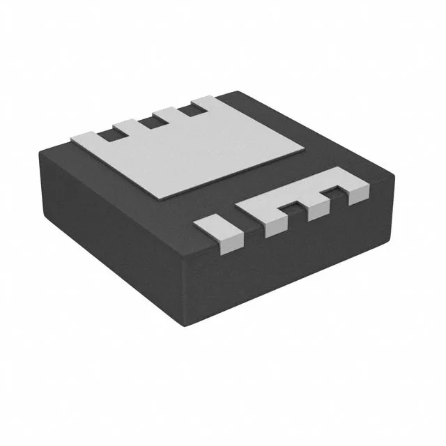
The pad is the main heat path — the datasheet shows 30 W dissipation at the case, but only 2.1 W in still air on a standard PCB. For rework, the exposed pad needs a hot-air profile that wets the pad fully without overheating the plastic body. The large thermal mass means a preheat at 150 °C helps avoid cold joints on the pad.
It is ROHS3 compliant.