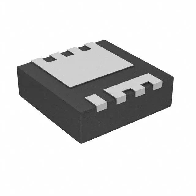
Infineon Technologies BSZ010NE2LS5ATMA1

Infineon BSZ010NE2LS5ATMA1 N-Ch MOSFET, 25 V, 1 mOhm

MPNBSZ010NE2LS5ATMA1
End of Life

Infineon OptiMOS™ 5 BSZ010NE2LS5ATMA1, N-Channel MOSFET, 25 V Vdss, 40 A continuous drain, 1 mOhm Rds(on) at 10 V, PG-TSDSON-8-FL package, -55 to 150 °C junction.

$2.79Ref. price · indicative, final on quote
Packaging8-PowerTDFN
StockContact for availability
MOQ1 pcs
  • 100% new & originalTraceable channels only — no refurbs, no pulls, no remarked parts.
  • Date & lot codes on quoteStated per line before you commit; label photos on request.
  • MSL-compliant ESD packingMoisture-sealed bags with indicator cards; reels photo-verified.
  • PayPal buyer protectionPay by T/T, PayPal or Payoneer — card payments covered end to end.

Specifications

BSZ010NE2LS5ATMA1 Technical Specifications
ParameterValue
SeriesOptiMOS™ 5
FET typeN-Channel
Mounting typeSurface Mount
Drain to source voltage25 V
Drive voltage (Max rds on, min rds on)4.5V, 10V
Current - continuous drain (Id) @ 25°C32A (Ta), 40A (Tc)
Power dissipation2.1W (Ta), 69W (Tc)
Operating temperature-55°C ~ 150°C (TJ)
PackageTape & Reel (TR); Cut Tape (CT)
Vgs±16V
TechnologyMOSFET (Metal Oxide)
Case8-PowerTDFN
Vgs(th) (Max) @ id2V @ 250µA
Rds on (Max) @ id, vgs1mOhm @ 20A, 10V
Gate charge (Qg) (Max) @ vgs29 nC @ 4.5 V
Input capacitance (Ciss) (Max) @ vds3900 pF @ 12 V

Product details

What this OptiMOS 5 part is and where it fits

The Infineon BSZ010NE2LS5ATMA1 is an N-channel power MOSFET from the OptiMOS™ 5 family, built on a metal-oxide trench technology. It handles a 25 V drain-to-source voltage and delivers up to 40 A continuous drain current at the case (Tc), with a 32 A rating at ambient (Ta). The headline number is the 1 mOhm maximum on-resistance at 10 V gate drive and 20 A — that milliohm figure keeps conduction losses low in a 12 V or 5 V rail, which is exactly where this part gets used: synchronous buck converters, load switches, battery protection, and OR-ing diodes in telecom or industrial gear. The junction temperature range of -55°C to 150°C means it can sit in an engine bay or a cold outdoor enclosure without derating surprises.

Package and mounting

At 20 A and 10 V gate drive, the drain-to-source resistance is guaranteed at 1 mOhm max. The PG-TSDSON-8-FL package can sink conduction loss to the PCB copper through its exposed pad.

Package and mounting — PG-TSDSON-8-FL

The 8-PowerTDFN case (Infineon calls it PG-TSDSON-8-FL) is a surface-mount package with a large drain pad on the bottom. That pad is the primary thermal path — it needs a good solder joint to a copper plane on the PCB, preferably with thermal vias to inner layers. The part is rated for 2.1 W dissipation in still air at the board level and 69 W when the case is held at 25°C, so the board layout determines how much current you can actually push. For a 40 A design, expect a multi-layer board with at least 2 oz copper and a dedicated thermal land. The package is compatible with standard reflow profiles; no special handling beyond normal MSL precautions.

Lifecycle and sourcing posture

The BSZ010NE2LS5ATMA1 carries an Active product status from Infineon and is ROHS3 compliant. No last-time-buy or NRND flags are on record.

Frequently asked questions

What is the gate charge and why does it matter?

The maximum gate charge is 29 nC at 4.5 V. That low Qg means the gate driver does not need to supply much current to switch the FET quickly — important for keeping switching losses down in a high-frequency converter.