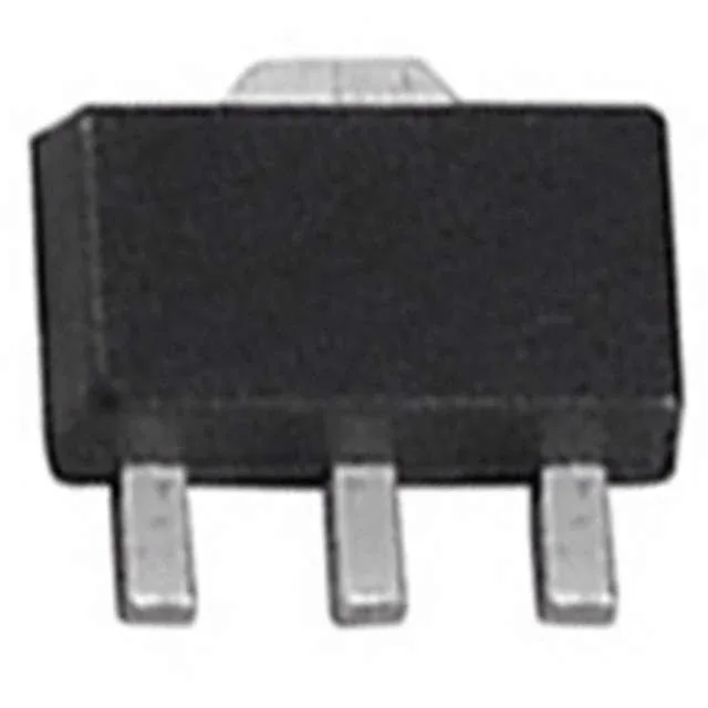
Infineon Technologies BSS87H6327FTSA1

Infineon BSS87H6327FTSA1 N-Ch MOSFET, 240 V, 260 mA, SOT-89

MPNBSS87H6327FTSA1
End of Life

Infineon SIPMOS® BSS87H6327FTSA1, N-Channel MOSFET, 240 Vdss, 260 mA continuous drain, 6 Ohm Rds(on) at 10 V, SOT-89 (PG-SOT89-4-2) surface-mount package, -55°C to 150°C junction temperature.

$0.58Ref. price · indicative, final on quote
PackagingTO-243AA
StockContact for availability
MOQ1 pcs
  • 100% new & originalTraceable channels only — no refurbs, no pulls, no remarked parts.
  • Date & lot codes on quoteStated per line before you commit; label photos on request.
  • MSL-compliant ESD packingMoisture-sealed bags with indicator cards; reels photo-verified.
  • PayPal buyer protectionPay by T/T, PayPal or Payoneer — card payments covered end to end.

Specifications

BSS87H6327FTSA1 Technical Specifications
ParameterValue
SeriesSIPMOS®
FET typeN-Channel
Mounting typeSurface Mount
Drain to source voltage240 V
Drive voltage (Max rds on, min rds on)4.5V, 10V
Current - continuous drain (Id) @ 25°C260mA (Ta)
Power dissipation1W (Ta)
Operating temperature-55°C ~ 150°C (TJ)
PackageTape & Reel (TR); Cut Tape (CT)
Vgs±20V
TechnologyMOSFET (Metal Oxide)
CaseTO-243AA
Vgs(th) (Max) @ id1.8V @ 108µA
Rds on (Max) @ id, vgs6Ohm @ 260mA, 10V
Gate charge (Qg) (Max) @ vgs5.5 nC @ 10 V
Input capacitance (Ciss) (Max) @ vds97 pF @ 25 V

Product details

240 V small-signal switch in a SOT-89 footprint

The Infineon BSS87H6327FTSA1 is an N-channel enhancement-mode MOSFET from the SIPMOS® family, rated for 240 V drain-to-source and 260 mA continuous drain current. The SOT-89 (PG-SOT89-4-2) package keeps the board footprint compact — the centre tab is the drain, and the copper area under it sets the thermal resistance to ambient for the 1 W power dissipation limit.

The 240 V Vdss gives headroom for 48 V, 72 V, and 120 V DC rails in industrial control, auxiliary power supplies, and telecom line cards — the 150°C junction rating means it can sit near a hot transformer or heatsink without derating the voltage. The 6 Ohm Rds(on) at 10 V gate drive is moderate for a 240 V device; at 260 mA the conduction loss is about 0.4 W, which fits within the 1 W package limit when the board has reasonable copper area. The 1.8 V typical gate threshold at 108 µA means the device can be driven from a 3.3 V logic output with a series gate resistor — the 4.5 V minimum drive voltage for the rated Rds(on) is the practical floor for full enhancement.

Temperature range and environment

The 150°C upper limit allows the device to operate near a 125°C ambient with the 1 W dissipation budget, provided the board layout pulls heat away from the SOT-89 tab.

Frequently asked questions

Is BSS87H6327FTSA1 RoHS compliant?

Yes, the BSS87H6327FTSA1 is ROHS3 compliant, meaning it meets the EU RoHS directive without exemptions for lead, mercury, cadmium, or other restricted substances.

Can BSS87H6327FTSA1 replace a standard BSS87?

The BSS87H6327FTSA1 is the same base die as the standard BSS87 but in a tape-and-reel packaging variant (H6327 suffix). The electrical ratings — 240 V Vdss, 260 mA Id, 6 Ohm Rds(on) — are identical. The package is the same SOT-89 (PG-SOT89-4-2), so it is a drop-in replacement for the standard BSS87 in surface-mount designs.

What is the maximum power dissipation of BSS87H6327FTSA1?

The maximum power dissipation is 1 W at 25°C ambient, measured with the device mounted on a standard FR-4 board. Derate above 25°C per the thermal resistance — the SOT-89 tab needs a copper pad area to keep the junction below 150°C at the full 1 W.

What is the lead time for BSS87H6327FTSA1?

Lead time is confirmed at quote time against the specific BOM quantity.