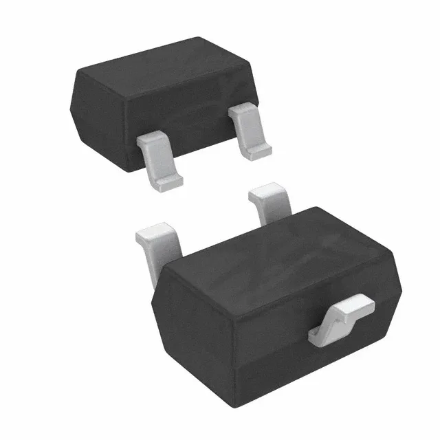
Infineon Technologies BSS816NWH6327XTSA1

Infineon BSS816NWH6327XTSA1 N-Ch MOSFET, 20 V, 1.4 A, SOT323

MPNBSS816NWH6327XTSA1
End of Life

Infineon OptiMOS™ BSS816NWH6327XTSA1, N-Channel MOSFET, 20 V drain-source, 1.4 A continuous, 160 mOhm Rds(on) at 2.5 V, 0.6 nC gate charge, SOT323-3 surface-mount package.

$0.48Ref. price · indicative, final on quote
PackagingSC-70, SOT-323
StockContact for availability
MOQ1 pcs
  • 100% new & originalTraceable channels only — no refurbs, no pulls, no remarked parts.
  • Date & lot codes on quoteStated per line before you commit; label photos on request.
  • MSL-compliant ESD packingMoisture-sealed bags with indicator cards; reels photo-verified.
  • PayPal buyer protectionPay by T/T, PayPal or Payoneer — card payments covered end to end.

Specifications

BSS816NWH6327XTSA1 Technical Specifications
ParameterValue
SeriesOptiMOS™
FET typeN-Channel
Mounting typeSurface Mount
Drain to source voltage20 V
Drive voltage (Max rds on, min rds on)1.8V, 2.5V
Current - continuous drain (Id) @ 25°C1.4A (Ta)
Power dissipation500mW (Ta)
Operating temperature-55°C ~ 150°C (TJ)
PackageTape & Reel (TR); Cut Tape (CT)
Vgs±8V
TechnologyMOSFET (Metal Oxide)
CaseSC-70, SOT-323
Vgs(th) (Max) @ id750mV @ 3.7µA
Rds on (Max) @ id, vgs160mOhm @ 1.4A, 2.5V
Gate charge (Qg) (Max) @ vgs0.6 nC @ 2.5 V
Input capacitance (Ciss) (Max) @ vds180 pF @ 10 V

Product details

160 mOhm Rds(on) in a SOT323 — load-switch and rail-switch fit

The 160 mOhm maximum on-resistance is specified at 1.4 A with a 2.5 V gate drive, meaning it turns on hard from a 2.5 V logic rail — no separate gate driver needed for most low-side or load-switch duty. The gate charge is only 0.6 nC at 2.5 V, so a microcontroller GPIO can switch it at moderate frequencies without excessive drive current. Input capacitance is 180 pF at 10 V drain-source, keeping the switching losses low in a 100–500 kHz DC-DC converter.

Thermal budget at 500 mW — what the SOT323 can sink

The package dissipates 500 mW at 25°C ambient (Ta). With 160 mOhm Rds(on) and 1.4 A, the conduction loss is I²R = 1.4² × 0.16 = 0.31 W, leaving about 190 mW of headroom for switching losses and ambient temperature rise. In a 70°C environment, derate the power by the SOT323 thermal resistance — expect the usable continuous current to drop to around 1.0 A. The operating junction temperature range is -55°C to 150°C, covering automotive under-hood and industrial extended-temperature enclosures. The PG-SOT323 supplier package is a standard 3-lead SOT-323 footprint, compatible with the common SC-70 land pattern.

Gate drive and switching — 1.8 V threshold, ±8 V max

The gate threshold voltage is 750 mV maximum at 3.7 µA drain current, and the drive voltage for minimum Rds(on) is 2.5 V. The part is fully rated for 1.8 V logic drive (the max Rds(on) condition), making it usable in 1.8 V systems like battery-powered IoT nodes or low-voltage FPGA I/O banks. The absolute maximum gate-source voltage is ±8 V, so 5 V logic is safe, but 12 V gate drive is not — stay within the ±8 V rail.

Lifecycle and procurement posture

No official second-source or pin-compatible alternate is listed on the Infineon cross-reference for this exact order code.

Frequently asked questions

What is the closest alternative to BSS816NWH6327XTSA1?

The OptiMOS™ family includes other SOT323 N-channel parts with similar voltage and current ratings, but pinout and threshold voltages vary — confirm the BOM position before substituting.