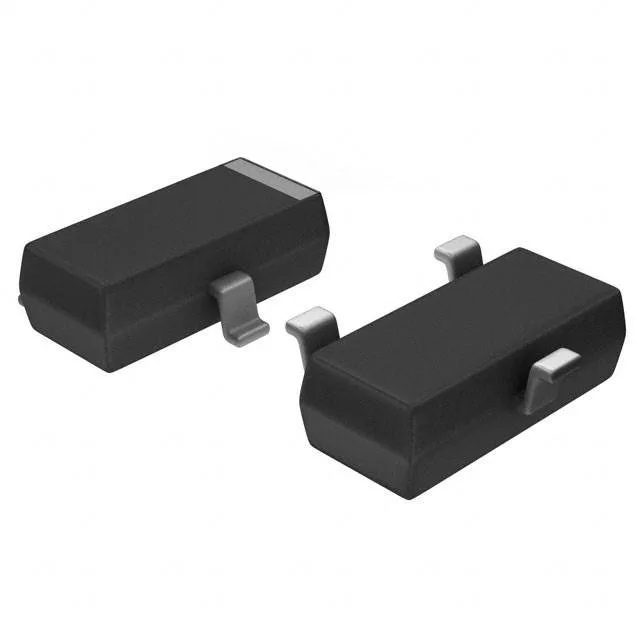
Infineon Technologies BSS806NEH6327XTSA1

BSS806NEH6327XTSA1 N-Channel MOSFET, 20 V, 2.3 A, SOT-23

MPNBSS806NEH6327XTSA1
End of Life

Infineon HEXFET® series BSS806NEH6327XTSA1, N-Channel MOSFET, 20 V Vdss, 2.3 A continuous drain, 57 mOhm Rds(on) at 2.5 V, PG-SOT23 package, AEC-Q101 qualified, -55 to 150 °C operating range.

$0.44Ref. price · indicative, final on quote
PackagingTO-236-3, SC-59, SOT-23-3
RoHSROHS3 Compliant
SeriesAutomotive, AEC-Q101, HEXFET®
Independent supplier — new & surplus stockAuthenticity-screened · ESD-safe packingListing updated Jul 2026

Specifications

BSS806NEH6327XTSA1 specifications
ParameterValue
SeriesAutomotive, AEC-Q101, HEXFET®
FET typeN-Channel
MountingSurface Mount
Drain to source voltage20 V
Drive voltage (Max rds on, min rds on)1.8V, 2.5V
Current - continuous drain (Id) @ 25°C2.3A (Ta)
Power dissipation500mW (Ta)
Operating temperature-55°C ~ 150°C (TJ)
PackageTape & Reel (TR); Cut Tape (CT)
Vgs±8V
TechnologyMOSFET (Metal Oxide)
CaseTO-236-3, SC-59, SOT-23-3
Vgs(th) (Max) @ id750mV @ 11µA
Rds on (Max) @ id, vgs57mOhm @ 2.3A, 2.5V
Gate charge (Qg) (Max) @ vgs1.7 nC @ 2.5 V
Input capacitance (Ciss) (Max) @ vds529 pF @ 10 V

Product details

57 mOhm at 2.5 V gate drive — what it buys the low-voltage rail

The headline spec is the 57 mOhm maximum on-resistance at 2.5 V gate drive — this means the part turns on hard from a 3.3 V or 1.8 V logic rail without needing a separate gate driver boost stage. It is built for low-voltage load switching, DC-DC converter synchronous rectification, and power distribution in automotive body electronics and industrial control modules.

AEC-Q101 and the 150 °C junction ceiling

Qualified to AEC-Q101, the part is screened for automotive-grade reliability — thermal cycling, high-temperature reverse bias, and humidity stress. The 500 mW power dissipation at 25 °C ambient in the SOT-23 package limits continuous current in still air; the 2.3 A rating assumes adequate PCB copper for heat spreading.

Gate charge and drive compatibility

Total gate charge is 1.7 nC at 2.5 V, with a maximum gate threshold of 750 mV at 11 µA. The low Qg allows direct PWM drive from a microcontroller GPIO at switching frequencies up to several hundred kilohertz without significant gate-drive losses. Input capacitance is 529 pF at 10 V drain bias, which keeps the Miller plateau short and reduces cross-conduction risk during fast edge transitions.

Supplied in the PG-SOT23 package (TO-236-3 / SC-59 / SOT-23-3 footprint), surface-mount. The 0.50 mm pitch and low profile suit dense PCB layouts in automotive ECU and portable equipment designs.

Frequently asked questions

What is the BSS806NEH6327XTSA1's gate drive voltage requirement?

The on-resistance is specified at 2.5 V gate drive, with a minimum drive voltage of 1.8 V for achieving the rated Rds(on). The maximum gate-source voltage is ±8 V.