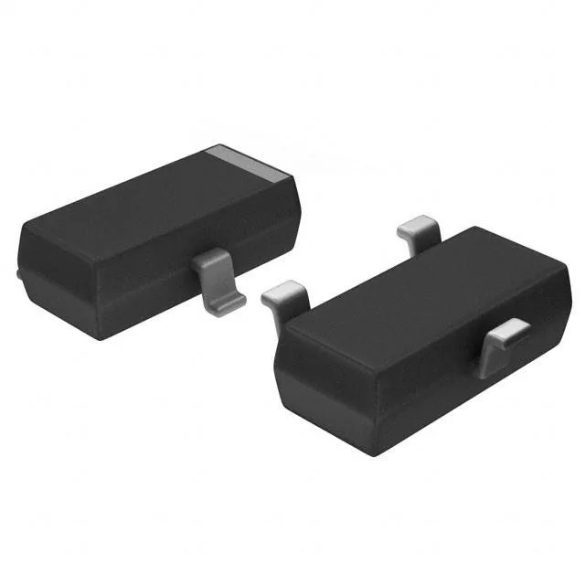
Infineon Technologies BSS215PH6327XTSA1

BSS215PH6327XTSA1 P-Channel MOSFET, 20 V, 1.5 A, SOT-23-3

MPNBSS215PH6327XTSA1
End of Life

Infineon OptiMOS™ BSS215PH6327XTSA1, P-Channel MOSFET, 20 V Vdss, 1.5 A continuous drain, 150 mOhm Rds(on) at 4.5 V, SOT-23-3 (PG-SOT23) surface-mount package, -55°C to 150°C junction temperature range.

$0.41Ref. price · indicative, final on quote
PackagingTO-236-3, SC-59, SOT-23-3
StockContact for availability
MOQ1 pcs
  • 100% new & originalTraceable channels only — no refurbs, no pulls, no remarked parts.
  • Date & lot codes on quoteStated per line before you commit; label photos on request.
  • MSL-compliant ESD packingMoisture-sealed bags with indicator cards; reels photo-verified.
  • PayPal buyer protectionPay by T/T, PayPal or Payoneer — card payments covered end to end.

Specifications

BSS215PH6327XTSA1 Technical Specifications
ParameterValue
SeriesOptiMOS™
FET typeP-Channel
Mounting typeSurface Mount
Drain to source voltage20 V
Drive voltage (Max rds on, min rds on)2.5V, 4.5V
Current - continuous drain (Id) @ 25°C1.5A (Ta)
Power dissipation500mW (Ta)
Operating temperature-55°C ~ 150°C (TJ)
PackageTape & Reel (TR); Cut Tape (CT)
Vgs±12V
TechnologyMOSFET (Metal Oxide)
CaseTO-236-3, SC-59, SOT-23-3
Vgs(th) (Max) @ id1.2V @ 11µA
Rds on (Max) @ id, vgs150mOhm @ 1.5A, 4.5V
Gate charge (Qg) (Max) @ vgs3.6 nC @ 4.5 V
Input capacitance (Ciss) (Max) @ vds346 pF @ 15 V

Product details

P-channel load switch for 20 V rails

The Infineon BSS215PH6327XTSA1 is a P-Channel enhancement-mode MOSFET from the OptiMOS™ family, rated for a maximum drain-to-source voltage of 20 V and a continuous drain current of 1.5 A at 25°C ambient. It comes in a standard SOT-23-3 surface-mount package, identified as the PG-SOT23 supplier device package. This part is designed for low-voltage load switching, battery protection, and power management in space-constrained designs where a P-channel device simplifies the gate drive by switching the high side without a charge pump.

On-resistance and gate drive — what 150 mOhm at 4.5 V means

The maximum on-resistance is 150 mOhm when the gate is driven to 4.5 V with 1.5 A of drain current. That 4.5 V drive level is typical of a 5 V logic output or a 3.3 V system with a level shifter — the part also specifies drive down to 2.5 V for minimum Rds(on), though the on-resistance will be higher at that lower gate voltage. For a 1 A load at 4.5 V drive, conduction loss is roughly 150 mW, which stays within the 500 mW power dissipation limit at 25°C ambient. The gate charge is only 3.6 nC at 4.5 V, so a GPIO pin can switch it directly without a dedicated gate driver.

Temperature range and environment

The 150°C maximum junction temperature gives headroom for self-heating in a high-ambient application, but the SOT-23-3 package limits total power dissipation to 500 mW at 25°C ambient, with derating above that temperature.

Frequently asked questions

Is BSS215PH6327XTSA1 obsolete or still in production?

Determines if the part can be sourced long-term or requires a redesign.

What is the price of BSS215PH6327XTSA1 in reel quantities?

Buyers need cost data for BOM budgeting and procurement decisions.

Where can I buy BSS215PH6327XTSA1 with stock today?

Immediate sourcing needs for production or repair require real-time inventory check.

What is the equivalent or replacement for BSS215PH6327XTSA1?

Engineers need drop-in alternatives for second sourcing or if part is unavailable.

What is the pinout and package of BSS215PH6327XTSA1?

Design validation requires correct footprint and pin mapping for layout.

Does BSS215PH6327XTSA1 have lead-free / RoHS compliance?

Environmental compliance is mandatory for many industries, especially EU markets.