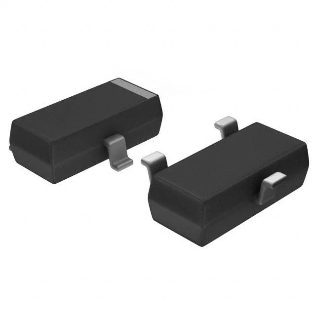
Infineon Technologies BSS159NH6327XTSA2

BSS159NH6327XTSA2 SIPMOS® N-Channel Depletion MOSFET, 60V

MPNBSS159NH6327XTSA2
End of Life

Infineon SIPMOS® series, N-Channel Depletion Mode MOSFET, 60 V Drain-Source Voltage, 230 mA Continuous Drain Current, 3.5 Ohm On-Resistance at 160 mA, 10 V, SOT-23-3 Package, -55°C to 150°C Operating Temperature.

$0.5Ref. price · indicative, final on quote
PackagingTO-236-3, SC-59, SOT-23-3
StockContact for availability
MOQ1 pcs
  • 100% new & originalTraceable channels only — no refurbs, no pulls, no remarked parts.
  • Date & lot codes on quoteStated per line before you commit; label photos on request.
  • MSL-compliant ESD packingMoisture-sealed bags with indicator cards; reels photo-verified.
  • PayPal buyer protectionPay by T/T, PayPal or Payoneer — card payments covered end to end.

Specifications

BSS159NH6327XTSA2 Technical Specifications
ParameterValue
SeriesSIPMOS®
FET typeN-Channel
Mounting typeSurface Mount
Drain to source voltage60 V
Drive voltage (Max rds on, min rds on)0V, 10V
Current - continuous drain (Id) @ 25°C230mA (Ta)
Power dissipation360mW (Ta)
Operating temperature-55°C ~ 150°C (TJ)
PackageTape & Reel (TR); Cut Tape (CT)
Vgs±20V
TechnologyMOSFET (Metal Oxide)
FET featureDepletion Mode
CaseTO-236-3, SC-59, SOT-23-3
Vgs(th) (Max) @ id2.4V @ 26µA
Rds on (Max) @ id, vgs3.5Ohm @ 160mA, 10V
Gate charge (Qg) (Max) @ vgs1.4 nC @ 5 V
Input capacitance (Ciss) (Max) @ vds39 pF @ 25 V

Product details

Depletion-mode small-signal switch for normally-on circuits

The Infineon BSS159NH6327XTSA2 is an N-channel depletion-mode MOSFET from the SIPMOS® family, packaged in a SOT-23-3 surface-mount case. Unlike enhancement-mode FETs, this device conducts current with zero gate voltage and requires a negative Vgs to pinch off — a characteristic useful for normally-on loads, current-source biasing, or fail-safe circuits where the load must stay powered if the gate drive is lost. Rated for 60 V drain-source and 230 mA continuous drain current at 25°C, it handles low-power switching and linear regulation in industrial, automotive, and telecom environments across a -55°C to 150°C junction temperature range.

On-resistance and gate drive — what the numbers mean for your circuit

Maximum on-resistance is 3.5 Ω at 160 mA drain current with 10 V applied to the gate. That Rds(on) is specified at a drive voltage of 10 V, but the part also supports a 0 V drive condition — the depletion-mode behaviour means the channel is fully on at zero gate bias. Gate charge is only 1.4 nC at 5 V, so the gate driver sees a light capacitive load; switching losses stay low even with a simple logic-level drive. Input capacitance is 39 pF at 25 V Vds, confirming this is a small-signal part suited for frequencies into the low-MHz range without excessive drive current.

Package and mounting

The SOT-23-3 (PG-SOT23) footprint is standard for low-power discretes. Power dissipation is limited to 360 mW at ambient temperature — adequate for signal-level switching but not for continuous high-current loads. The surface-mount package suits automated assembly and reflow processes common in high-volume production.

Lifecycle and sourcing

The BSS159NH6327XTSA2 carries an Active product status with ROHS3 compliance. No end-of-life notice or last-time-buy window is indicated.

Frequently asked questions

Where can I buy BSS159NH6327XTSA2?

This part is sourced to order through independent distribution. Submit an RFQ for current pricing and availability.