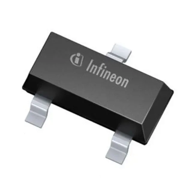
Infineon Technologies BSS123IXTMA1 — Discrete Semiconductors

Infineon BSS123IXTMA1 N-Channel MOSFET, 100 V, 190 mA

MPNBSS123IXTMA1
Active

Infineon OptiMOS™ N-Channel MOSFET, 100 V Vdss, 190 mA continuous drain (Ta), 6 Ohm Rds(on) @ 190 mA, 10 V, SOT-23-3, -55°C to 150°C TJ.

$0.4200Ref. price · indicative, final on quote
StockContact for availability
MOQ1 pcs
  • 100% new & originalTraceable channels only — no refurbs, no pulls, no remarked parts.
  • Date & lot codes on quoteStated per line before you commit; label photos on request.
  • MSL-compliant ESD packingMoisture-sealed bags with indicator cards; reels photo-verified.
  • PayPal buyer protectionPay by T/T, PayPal or Payoneer — card payments covered end to end.

Specifications

BSS123IXTMA1 Technical Specifications
ParameterValue
SeriesOptiMOS™
FET typeN-Channel
Mounting typeSurface Mount
Drain to source voltage100 V
Drive voltage (Max rds on, min rds on)4.5V, 10V
Current - continuous drain (Id) @ 25°C190mA (Ta)
Power dissipation500mW (Ta)
Operating temperature-55°C~150°C(TJ)
PackageTape & Reel (TR); Cut Tape (CT)
Vgs±20V
TechnologyMOSFET (Metal Oxide)
CaseTO-236-3, SC-59, SOT-23-3
Vgs(th) (Max) @ id1.8V @ 13µA
Rds on (Max) @ id, vgs6Ohm @ 190mA, 10V
Gate charge (Qg) (Max) @ vgs0.63 nC @ 10 V
Input capacitance (Ciss) (Max) @ vds15 pF @ 50 V

Product details

100 V N-channel in a SOT-23 — what it handles

The Infineon BSS123IXTMA1 is a 100 V N-channel enhancement-mode MOSFET from the OptiMOS series, built for low-power switching and load-management tasks where board space is tight.

Gate drive and switching — logic-level compatibility

With a maximum gate threshold voltage of 1.8 V at 13 µA, this part turns on cleanly from 3.3 V logic rails, though the drive voltage range for rated Rds(on) is 4.5 V to 10 V. The gate charge is only 0.63 nC at 10 V, and input capacitance measures 15 pF at 50 V drain bias — both low enough for direct GPIO drive in moderate-speed switching up to a few hundred kHz. The ±20 V maximum gate-source rating gives margin for ringing on long traces.

Package and power dissipation

Maximum power dissipation is 500 mW at 25°C ambient (Ta), typical for a SOT-23-3 device. The small footprint means thermal management relies on the PCB copper; for continuous loads near the 190 mA limit, ensure adequate trace width and via stitching to the ground plane.

Lifecycle and sourcing

The base product number is BSS123, and the IXTMA1 suffix denotes the specific reel and packaging variant.

Frequently asked questions

Is BSS123IXTMA1 equivalent to BSS123?

Yes. BSS123IXTMA1 is a specific packaging and reel variant of the base BSS123 device. The electrical specifications — 100 V Vdss, 190 mA continuous drain, 6 Ohm Rds(on) at 10 V — are identical to the standard BSS123. The IXTMA1 suffix indicates the Tape & Reel format and Infineon's internal ordering code.

What is the Rds(on) of BSS123IXTMA1?

The maximum on-resistance is 6 Ohm at a drain current of 190 mA and 10 V gate drive. At 4.5 V gate drive the Rds(on) will be higher, so for logic-level operation at 3.3 V, verify the drive voltage against the gate threshold and expected load current.